Free Access
Fig. 4
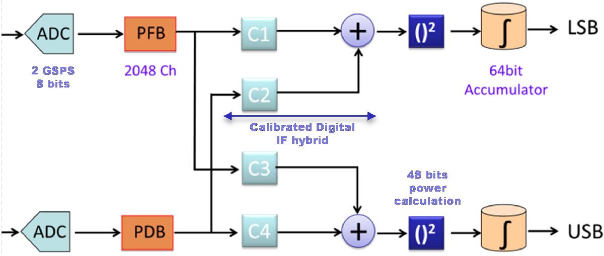
FPGA firmware top-level block diagram. From left to right main subsystems are: ADC hardware interface, Polyphase Filter Bank (PFB), Complex vector multipliers (C1–C4), Complex Adders (+), Power blocks ()2, and vector accumulators.
Current usage metrics show cumulative count of Article Views (full-text article views including HTML views, PDF and ePub downloads, according to the available data) and Abstracts Views on Vision4Press platform.
Data correspond to usage on the plateform after 2015. The current usage metrics is available 48-96 hours after online publication and is updated daily on week days.
Initial download of the metrics may take a while.