| Issue |
A&A
Volume 707, March 2026
|
|
|---|---|---|
| Article Number | A230 | |
| Number of page(s) | 25 | |
| Section | Astronomical instrumentation | |
| DOI | https://doi.org/10.1051/0004-6361/202555777 | |
| Published online | 17 March 2026 | |
Euclid preparation
LXXX. Overview of Euclid infrared detector performance from ground tests
1
Université Claude Bernard Lyon 1, CNRS/IN2P3, IP2I Lyon,
UMR 5822,
Villeurbanne
69100,
France
2
Aix-Marseille Université, CNRS/IN2P3, CPPM,
Marseille,
France
3
ESAC/ESA, Camino Bajo del Castillo, s/n., Urb. Villafranca del Castillo,
28692
Villanueva de la Cañada, Madrid,
Spain
4
European Space Agency/ESTEC,
Keplerlaan 1,
2201
AZ
Noordwijk,
The Netherlands
5
European Space Agency/ESRIN,
Largo Galileo Galilei 1,
00044
Frascati, Roma,
Italy
6
Centre National d’Etudes Spatiales – Centre spatial de Toulouse,
18 avenue Edouard Belin,
31401
Toulouse Cedex 9,
France
7
Jet Propulsion Laboratory, California Institute of Technology,
4800 Oak Grove Drive,
Pasadena,
CA
91109,
USA
8
NASA Goddard Space Flight Center,
Greenbelt,
MD
20771,
USA
9
Carnegie Observatories,
Pasadena,
CA
91101,
USA
10
Max-Planck-Institut für Astronomie,
Königstuhl 17,
69117
Heidelberg,
Germany
11
Max Planck Institute for Extraterrestrial Physics,
Giessenbachstr. 1,
85748
Garching,
Germany
12
Universitäts-Sternwarte München, Fakultät für Physik, Ludwig-Maximilians-Universität München,
Scheinerstrasse 1,
81679
München,
Germany
13
INAF-Osservatorio Astronomico di Padova,
Via dell’Osservatorio 5,
35122
Padova,
Italy
14
INAF-Osservatorio Astrofisico di Torino,
Via Osservatorio 20,
10025
Pino Torinese (TO),
Italy
15
INFN-Padova,
Via Marzolo 8,
35131
Padova,
Italy
16
INAF-Osservatorio di Astrofisica e Scienza dello Spazio di Bologna,
Via Piero Gobetti 93/3,
40129
Bologna,
Italy
17
Kapteyn Astronomical Institute, University of Groningen,
PO Box 800,
9700
AV
Groningen,
The Netherlands
18
Leiden Observatory, Leiden University,
Einsteinweg 55,
2333
CC
Leiden,
The Netherlands
19
Aix-Marseille Université, CNRS, CNES, LAM,
Marseille,
France
20
INFN-Bologna,
Via Irnerio 46,
40126
Bologna,
Italy
21
Dipartimento di Fisica e Astronomia “Augusto Righi” – Alma Mater Studiorum Università di Bologna,
via Piero Gobetti 93/2,
40129
Bologna,
Italy
22
Dipartimento di Fisica e Astronomia “G. Galilei”, Università di Padova,
Via Marzolo 8,
35131
Padova,
Italy
23
Universidad Politécnica de Cartagena, Departamento de Electrónica y Tecnología de Computadoras,
Plaza del Hospital 1,
30202
Cartagena,
Spain
24
INFN-Sezione di Bologna,
Viale Berti Pichat 6/2,
40127
Bologna,
Italy
25
Université Paris-Saclay, CNRS, Institut d’astrophysique spatiale,
91405
Orsay,
France
26
INAF-Osservatorio Astronomico di Brera,
Via Brera 28,
20122
Milano,
Italy
27
IFPU, Institute for Fundamental Physics of the Universe,
via Beirut 2,
34151
Trieste,
Italy
28
INAF-Osservatorio Astronomico di Trieste,
Via G. B. Tiepolo 11,
34143
Trieste,
Italy
29
INFN, Sezione di Trieste,
Via Valerio 2,
34127
Trieste
TS,
Italy
30
SISSA, International School for Advanced Studies,
Via Bonomea 265,
34136
Trieste
TS,
Italy
31
Dipartimento di Fisica e Astronomia, Università di Bologna,
Via Gobetti 93/2,
40129
Bologna,
Italy
32
Institut de Physique Théorique, CEA, CNRS, Université Paris-Saclay,
91191
Gif-sur-Yvette Cedex,
France
33
Institut d’Astrophysique de Paris, UMR 7095, CNRS, and Sorbonne Université,
98 bis boulevard Arago,
75014
Paris,
France
34
Space Science Data Center, Italian Space Agency, via del Politecnico snc,
00133
Roma,
Italy
35
Dipartimento di Fisica, Università di Genova,
Via Dodecaneso 33,
16146
Genova,
Italy
36
INFN-Sezione di Genova,
Via Dodecaneso 33,
16146
Genova,
Italy
37
Department of Physics “E. Pancini”, University Federico II,
Via Cinthia 6,
80126
Napoli,
Italy
38
INAF-Osservatorio Astronomico di Capodimonte,
Via Moiariello 16,
80131
Napoli,
Italy
39
Instituto de Astrofísica e Ciências do Espaço, Universidade do Porto, CAUP, Rua das Estrelas,
4150-762
Porto,
Portugal
40
Faculdade de Ciências da Universidade do Porto, Rua do Campo de Alegre,
4150-007
Porto,
Portugal
41
Dipartimento di Fisica, Università degli Studi di Torino,
Via P. Giuria 1,
10125
Torino,
Italy
42
INFN-Sezione di Torino,
Via P. Giuria 1,
10125
Torino,
Italy
43
Institute Lorentz, Leiden University,
Niels Bohrweg 2,
2333
CA
Leiden,
The Netherlands
44
INAF-IASF Milano,
Via Alfonso Corti 12,
20133
Milano,
Italy
45
Centro de Investigaciones Energéticas, Medioambientales y Tecnológicas (CIEMAT),
Avenida Complutense 40,
28040
Madrid,
Spain
46
Port d’Informació Científica, Campus UAB, C. Albareda s/n,
08193
Bellaterra (Barcelona),
Spain
47
Institute for Theoretical Particle Physics and Cosmology (TTK), RWTH Aachen University,
52056
Aachen,
Germany
48
Institute of Space Sciences (ICE, CSIC), Campus UAB, Carrer de Can Magrans, s/n,
08193
Barcelona,
Spain
49
Institut d’Estudis Espacials de Catalunya (IEEC), Edifici RDIT, Campus UPC,
08860
Castelldefels, Barcelona,
Spain
50
INAF-Osservatorio Astronomico di Roma,
Via Frascati 33,
00078
Monteporzio Catone,
Italy
51
INFN section of Naples,
Via Cinthia 6,
80126
Napoli,
Italy
52
Institute for Astronomy, University of Hawaii,
2680 Woodlawn Drive,
Honolulu,
HI
96822,
USA
53
Dipartimento di Fisica e Astronomia “Augusto Righi” – Alma Mater Studiorum Università di Bologna,
Viale Berti Pichat 6/2,
40127
Bologna,
Italy
54
Instituto de Astrofísica de Canarias, Vía Láctea,
38205
La Laguna, Tenerife,
Spain
55
Institute for Astronomy, University of Edinburgh, Royal Observatory, Blackford Hill,
Edinburgh
EH9 3HJ,
UK
56
Jodrell Bank Centre for Astrophysics, Department of Physics and Astronomy, University of Manchester,
Oxford Road,
Manchester
M13 9PL,
UK
57
Institut de Ciències del Cosmos (ICCUB), Universitat de Barcelona (IEEC-UB),
Martí i Franquès 1,
08028
Barcelona,
Spain
58
Institució Catalana de Recerca i Estudis Avançats (ICREA),
Passeig de Lluís Companys 23,
08010
Barcelona,
Spain
59
UCB Lyon 1, CNRS/IN2P3, IUF, IP2I Lyon,
4 rue Enrico Fermi,
69622
Villeurbanne,
France
60
Departamento de Física, Faculdade de Ciências, Universidade de Lisboa,
Edifício C8, Campo Grande,
1749-016
Lisboa,
Portugal
61
Instituto de Astrofísica e Ciências do Espaço, Faculdade de Ciências, Universidade de Lisboa, Campo Grande,
1749-016
Lisboa,
Portugal
62
Department of Astronomy, University of Geneva,
ch. d’Ecogia 16,
1290
Versoix,
Switzerland
63
INAF-Istituto di Astrofisica e Planetologia Spaziali,
via del Fosso del Cavaliere, 100,
00100
Roma,
Italy
64
School of Physics, HH Wills Physics Laboratory, University of Bristol,
Tyndall Avenue,
Bristol
BS8 1TL,
UK
65
Dipartimento di Fisica “Aldo Pontremoli”, Università degli Studi di Milano,
Via Celoria 16,
20133
Milano,
Italy
66
INFN-Sezione di Milano,
Via Celoria 16,
20133
Milano,
Italy
67
Institute of Theoretical Astrophysics, University of Oslo,
PO Box 1029 Blindern,
0315
Oslo,
Norway
68
Department of Physics, Lancaster University,
Lancaster
LA1 4YB,
UK
69
Felix Hormuth Engineering,
Goethestr. 17,
69181
Leimen,
Germany
70
Technical University of Denmark,
Elektrovej 327,
2800
Kgs. Lyngby,
Denmark
71
Cosmic Dawn Center (DAWN),
Denmark
72
Department of Physics and Helsinki Institute of Physics,
Gustaf Hällströmin katu 2,
00014
University of Helsinki,
Finland
73
Université de Genève, Département de Physique Théorique and Centre for Astroparticle Physics,
24 quai Ernest-Ansermet,
1211
Genève 4,
Switzerland
74
Department of Physics,
PO Box 64,
00014
University of Helsinki,
Finland
75
Helsinki Institute of Physics,
Gustaf Hällströmin katu 2, University of Helsinki,
Helsinki,
Finland
76
Centre de Calcul de 1’IN2P3/CNRS,
21 avenue Pierre de Coubertin
69627
Villeurbanne Cedex,
France
77
Laboratoire d’etude de l’Univers et des phenomenes eXtremes, Observatoire de Paris, Université PSL, Sorbonne Université, CNRS,
92190
Meudon,
France
78
Mullard Space Science Laboratory, University College London, Holmbury St Mary, Dorking,
Surrey
RH5 6NT,
UK
79
SKA Observatory, Jodrell Bank, Lower Withington, Macclesfield,
Cheshire
SK11 9FT,
UK
80
University of Applied Sciences and Arts of Northwestern Switzerland, School of Computer Science,
5210
Windisch,
Switzerland
81
Universität Bonn, Argelander-Institut für Astronomie,
Auf dem Hügel 71,
53121
Bonn,
Germany
82
INFN-Sezione di Roma,
Piazzale Aldo Moro 2, c/o Dipartimento di Fisica, Edificio G. Marconi,
00185
Roma,
Italy
83
Department of Physics, Institute for Computational Cosmology, Durham University,
South Road,
Durham
DH1 3LE,
UK
84
Université Côte d’Azur, Observatoire de la Côte d’Azur, CNRS, Laboratoire Lagrange,
Bd de l’Observatoire, CS 34229,
06304
Nice cedex 4,
France
85
Université Paris Cité, CNRS, Astroparticule et Cosmologie,
75013
Paris,
France
86
CNRS-UCB International Research Laboratory, Centre Pierre Binétruy, IRL2007, CPB-IN2P3,
Berkeley,
USA
87
University of Applied Sciences and Arts of Northwestern Switzerland, School of Engineering,
5210
Windisch,
Switzerland
88
Institut d’Astrophysique de Paris,
98bis Boulevard Arago,
75014,
Paris,
France
89
Institute of Physics, Laboratory of Astrophysics, Ecole Polytechnique Fédérale de Lausanne (EPFL), Observatoire de Sauverny,
1290
Versoix,
Switzerland
90
Aurora Technology for European Space Agency (ESA), Camino bajo del Castillo, s/n, Urbanizacion Villafranca del Castillo, Villanueva de la Cañada,
28692
Madrid,
Spain
91
California Institute of Technology,
1200 E California Blvd,
Pasadena,
CA
91125,
USA
92
Institut de Física d’Altes Energies (IFAE), The Barcelona Institute of Science and Technology, Campus UAB,
08193
Bellaterra (Barcelona),
Spain
93
School of Mathematics and Physics, University of Surrey, Guildford,
Surrey
GU2 7XH,
UK
94
DARK, Niels Bohr Institute, University of Copenhagen,
Jagtvej 155,
2200
Copenhagen,
Denmark
95
Waterloo Centre for Astrophysics, University of Waterloo, Waterloo,
Ontario
N2L 3G1,
Canada
96
Department of Physics and Astronomy, University of Waterloo, Waterloo,
Ontario
N2L 3G1,
Canada
97
Perimeter Institute for Theoretical Physics, Waterloo,
Ontario
N2L 2Y5,
Canada
98
Université Paris-Saclay, Université Paris Cité, CEA, CNRS, AIM,
91191,
Gif-sur-Yvette,
France
99
Institute of Space Science, Str. Atomistilor,
nr. 409 Măgurele,
Ilfov
077125,
Romania
100
Consejo Superior de Investigaciones Cientificas,
Calle Serrano 117,
28006
Madrid,
Spain
101
Universidad de La Laguna, Departamento de Astrofísica,
38206
La Laguna, Tenerife,
Spain
102
Institut für Theoretische Physik, University of Heidelberg,
Philosophenweg 16,
69120
Heidelberg,
Germany
103
Institut de Recherche en Astrophysique et Planétologie (IRAP), Université de Toulouse, CNRS, UPS, CNES,
14 Av. Edouard Belin,
31400
Toulouse,
France
104
Université St Joseph, Faculty of Sciences,
Beirut,
Lebanon
105
Departamento de Física, FCFM, Universidad de Chile, Blanco Encalada
2008,
Santiago,
Chile
106
Universität Innsbruck, Institut für Astro- und Teilchenphysik,
Technikerstr. 25/8,
6020
Innsbruck,
Austria
107
Satlantis, University Science Park,
Sede Bld
48940,
Leioa-Bilbao,
Spain
108
Infrared Processing and Analysis Center, California Institute of Technology,
Pasadena,
CA
91125,
USA
109
Instituto de Astrofísica e Ciências do Espaço, Faculdade de Ciências, Universidade de Lisboa, Tapada da Ajuda,
1349-018
Lisboa,
Portugal
110
Cosmic Dawn Center (DAWN)
111
Niels Bohr Institute, University of Copenhagen,
Jagtvej 128,
2200
Copenhagen,
Denmark
112
Centre for Information Technology, University of Groningen,
PO Box 11044,
9700
CA
Groningen,
The Netherlands
113
Dipartimento di Fisica e Scienze della Terra, Università degli Studi di Ferrara,
Via Giuseppe Saragat 1,
44122
Ferrara,
Italy
114
Istituto Nazionale di Fisica Nucleare, Sezione di Ferrara,
Via Giuseppe Saragat 1,
44122
Ferrara,
Italy
115
INAF, Istituto di Radioastronomia,
Via Piero Gobetti 101,
40129
Bologna,
Italy
116
Department of Physics, Oxford University,
Keble Road,
Oxford
OX1 3RH,
UK
117
INAF – Osservatorio Astronomico di Brera,
via Emilio Bianchi 46,
23807
Merate,
Italy
118
INAF-Osservatorio Astronomico di Brera, Via Brera 28, 20122 Milano Italy, and INFN-Sezione di Genova,
Via Dodecaneso 33,
16146
Genova,
Italy
119
ICL, Junia, Université Catholique de Lille, LITL,
59000
Lille,
France
120
ICSC – Centro Nazionale di Ricerca in High Performance Computing, Big Data e Quantum Computing,
Via Magnanelli 2,
Bologna,
Italy
121
Instituto de Física Teórica UAM-CSIC, Campus de Cantoblanco,
28049
Madrid,
Spain
122
CERCA/ISO, Department of Physics, Case Western Reserve University,
10900 Euclid Avenue,
Cleveland,
OH
44106,
USA
123
Technical University of Munich, TUM School of Natural Sciences, Physics Department,
James-Franck-Str. 1,
85748
Garching,
Germany
124
Max-Planck-Institut für Astrophysik,
Karl-Schwarzschild-Str. 1,
85748
Garching,
Germany
125
Laboratoire Univers et Théorie, Observatoire de Paris, Université PSL, Université Paris Cité, CNRS,
92190
Meudon,
France
126
Departamento de Física Fundamental. Universidad de Salamanca. Plaza de la Merced s/n,
37008
Salamanca,
Spain
127
Université de Strasbourg, CNRS, Observatoire astronomique de Strasbourg,
UMR 7550,
67000
Strasbourg,
France
128
Center for Data-Driven Discovery, Kavli IPMU (WPI), UTIAS, The University of Tokyo, Kashiwa,
Chiba
277-8583,
Japan
129
Dipartimento di Fisica – Sezione di Astronomia, Università di Trieste,
Via Tiepolo 11,
34131
Trieste,
Italy
130
University of California,
Los Angeles,
CA
90095-1562,
USA
131
Department of Physics & Astronomy, University of California Irvine,
Irvine,
CA
92697,
USA
132
Department of Mathematics and Physics E. De Giorgi, University of Salento, Via per Arnesano, CP-I93,
73100
Lecce,
Italy
133
INFN, Sezione di Lecce, Via per Arnesano, CP-193,
73100
Lecce,
Italy
134
INAF-Sezione di Lecce, c/o Dipartimento Matematica e Fisica, Via per Arnesano,
73100
Lecce,
Italy
135
Departamento Física Aplicada, Universidad Politécnica de Cartagena, Campus Muralla del Mar,
30202
Cartagena, Murcia,
Spain
136
Instituto de Física de Cantabria, Edificio Juan Jordá, Avenida de los Castros,
39005
Santander,
Spain
137
Observatorio Nacional, Rua General Jose Cristino,
77-Bairro Imperial de Sao Cristovao,
Rio de Janeiro
20921-400,
Brazil
138
CEA Saclay, DFR/IRFU, Service d’Astrophysique,
Bat. 709,
91191
Gif-sur-Yvette,
France
139
Institute of Cosmology and Gravitation, University of Portsmouth,
Portsmouth
PO1 3FX,
UK
140
Department of Computer Science, Aalto University,
PO Box 15400,
Espoo
00 076,
Finland
141
Instituto de Astrofísica de Canarias, c/ Via Lactea s/n, La Laguna 38200, Spain. Departamento de Astrofísica de la Universidad de La Laguna, Avda. Francisco Sanchez,
La Laguna
38200,
Spain
142
Ruhr University Bochum, Faculty of Physics and Astronomy, Astronomical Institute (AIRUB), German Centre for Cosmological Lensing (GCCL),
44780
Bochum,
Germany
143
Department of Physics and Astronomy,
Vesilinnantie 5,
20014
University of Turku,
Finland
144
Serco for European Space Agency (ESA), Camino bajo del Castillo, s/n, Urbanizacion Villafranca del Castillo, Villanueva de la Cañada,
28692
Madrid,
Spain
145
ARC Centre of Excellence for Dark Matter Particle Physics,
Melbourne,
Australia
146
Centre for Astrophysics & Supercomputing, Swinburne University of Technology, Hawthorn,
Victoria
3122,
Australia
147
Department of Physics and Astronomy, University of the Western Cape, Bellville,
Cape Town
7535,
South Africa
148
DAMTP, Centre for Mathematical Sciences,
Wilberforce Road,
Cambridge
CB3 0WA,
UK
149
Kavli Institute for Cosmology Cambridge,
Madingley Road,
Cambridge,
CB3 0HA,
UK
150
Department of Astrophysics, University of Zurich,
Winterthurerstrasse 190,
8057
Zurich,
Switzerland
151
Department of Physics, Centre for Extragalactic Astronomy, Durham University,
South Road,
Durham,
DH1 3LE,
UK
152
IRFU, CEA, Université Paris-Saclay,
91191
Gif-sur-Yvette Cedex,
France
153
Oskar Klein Centre for Cosmoparticle Physics, Department of Physics, Stockholm University,
Stockholm
S106 91,
Sweden
154
Astrophysics Group, Blackett Laboratory, Imperial College London,
London
SW7 2AZ,
UK
155
Univ. Grenoble Alpes, CNRS,
Grenoble INP, LPSC-IN2P3, 53, Avenue des Martyrs,
38000
Grenoble,
France
156
INAF-Osservatorio Astrofisico di Arcetri,
Largo E. Fermi 5,
50125
Firenze,
Italy
157
Dipartimento di Fisica, Sapienza Università di Roma,
Piazzale Aldo Moro 2,
00185
Roma,
Italy
158
Centro de Astrofísica da Universidade do Porto, Rua das Estrelas
4150-762
Porto,
Portugal
159
HE Space for European Space Agency (ESA), Camino bajo del Castillo, s/n, Urbanizacion Villafranca del Castillo, Villanueva de la Cañada,
28692
Madrid,
Spain
160
Theoretical astrophysics, Department of Physics and Astronomy, Uppsala University,
Box 516,
751 37
Uppsala,
Sweden
161
Mathematical Institute, University of Leiden,
Einsteinweg 55,
2333
CA
Leiden,
The Netherlands
162
Institute of Astronomy, University of Cambridge,
Madingley Road,
Cambridge
CB3 0HA,
UK
163
Department of Astrophysical Sciences, Peyton Hall, Princeton University,
Princeton,
NJ
08544,
USA
164
Space physics and astronomy research unit, University of Oulu,
Pentti Kaiteran katu 1,
90014
Oulu,
Finland
165
Center for Computational Astrophysics, Flatiron Institute,
162 5th Avenue,
10010,
New York,
NY,
USA
166
Department of Astronomy, University of Massachusetts,
Amherst,
MA
01003,
USA
★ Corresponding author: This email address is being protected from spambots. You need JavaScript enabled to view it.
Received:
2
June
2025
Accepted:
6
October
2025
Abstract
This paper describes the objectives, design, and findings of the pre-launch ground characterisation campaigns of the Euclid infrared detectors. The aim of the ground characterisations is to evaluate the performance of the detectors, to calibrate the pixel response, and to derive the pixel response correction methods. The detectors have been tested and characterised in the facilities set up for this purpose. The pixel properties, including baseline, bad pixels, quantum efficiency, inter pixel capacitance, quantum efficiency, dark current, readout noise, conversion gain, response non-linearity, and image persistence were measured and characterised for each pixel. We describe in detail the test flow definition that allows us to derive the pixel properties and we present the data acquisition and data quality check software implemented for this purpose. We also outline the measurement protocols of all the pixel properties presented and we provide a comprehensive overview of the performance of the Euclid infrared detectors as derived after tuning the operating parameters of the detectors. The main conclusion of this work is that the performance of the infrared detectors Euclid meets the requirements. Pixels classified as non-functioning accounted for less than 0.2% of all science pixels. The interpixel capacitance (IPC) coupling is minimal, the cross-talk between adjacent pixels is less than 1% between adjacent pixels, and 95% of the pixels show a quantum efficienty (QE) greater than 80% across the entire spectral range of the Euclid mission. The conversion gain is approximately 0.52 ADU/e−, with a variation of less than 1% between channels of the same detector. The reset noise is approximately equal to 23 ADU rms after reference pixel correction. The readout noise of a single frame is approximately 13 e− rms while the signal estimator noise is measured at 7 e− rms in photometric mode and 9 e− rms in spectroscopic acquisition mode. The deviation from linear response at signal levels up to 80 ke− is less than 5% for 95% of the pixels. Median persistence amplitudes are less than 0.3% of the signal, though persistence exhibits significant spatial variation and differences between detectors.
Key words: instrumentation: detectors / methods: data analysis / space vehicles: instruments
© The Authors 2026
 Open Access article, published by EDP Sciences, under the terms of the Creative Commons Attribution License (https://creativecommons.org/licenses/by/4.0), which permits unrestricted use, distribution, and reproduction in any medium, provided the original work is properly cited.
This article is published in open access under the Subscribe to Open model. This email address is being protected from spambots. You need JavaScript enabled to view it. to support open access publication.
1 Introduction
The Euclid mission, led by the European Space Agency (ESA) in collaboration with NASA, represents a cornerstone in our quest to understand the nature of dark energy and dark matter (Laureijs et al. 2011; Euclid Collaboration: Mellier 2025). With its wide field of view of 0.5 deg2, the Euclid telescope will scan 14 000 deg2 of the extragalactic sky from the second Sun–Earth Lagrange point (Euclid Collaboration: Scaramella 2022).
Equipped with two cutting-edge instruments – the visible imager VIS (Euclid Collaboration: Cropper 2025) and the Near Infrared Spectrometer and Photometer (NISP; Euclid Collaboration: Jahnke 2025) – the aim of the mission is to map the geometry of the Universe with unprecedented precision. Central to the success of NISP is its reliance on HAWAII-2RG (H2RG)1 detector arrays whose characterisation and calibration are crucial for ensuring scientific accuracy.
Achieving the ambitious observational goals of the Euclid telescope depends on reduced instrument systematics and precise measurements from the detectors. To maximise the performance of the detection chain signal, we must generally maximise the observed signal and minimise any sources of noise. To do this, we need detectors with high quantum efficiency (QE), low dark current and low readout noise. Likewise, we want devices with low persistence because the false current from the previous exposures would also contribute to noise and is difficult to model and remove. At the same time, the capacitive couplings between pixels should be minimal because they affect the instrument’s point spread function (PSF).
With the increasing demand for low-signal observations and the growing complexity of scientific requirements, achieving higher precision in detector performance measurements is becoming more critical. The ground characterisation performed in 2019 by the NISP detector team focuses on calibrating pixel responses and creating pixel maps that account for both systematic errors and correction functions. These functions correct for effects arising in the detector, ensuring the reliability of scientific data.
This paper presents the methodology of characterisation and summarises the key properties of the flight detectors. In Sect. 2 we present the architecture of the detector system, the detector readout principle, the common-mode correction approach, as well as the signal estimation algorithm employed during the Euclid mission and in the generation of calibration products. In Sect. 3 we outline the objectives of the characterisation campaign, detail and motivate the steps of the test-flow and describe the software developed for automated data acquisition and verification. Section 4 presents the procedure of tuning the fundamental parameters of the detector system. The main results are presented in Sect. 5, which provides a comprehensive overview of all detector properties measured during ground tests. For each property, we begin by explaining its physical significance and role in the overall performance of the detector system. Next, the specific measurement protocols used to evaluate each property are discussed, outlining the steps taken to ensure accuracy and consistency. The measurement results are then presented, highlighting their potential implications for detector performance. Section 6 summarises the obtained results. A summary table of the main detector properties is given in Appendix A. Appendix B presents the formalism of orthogonal polynomials employed in the non-linearity characterisation.
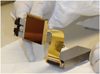 |
Fig. 1 Photo of a Euclid-like engineering grade sensor chip system taken in the clean room of the CNRS-IN2P3 Center for Particle Physics in Marseille (CPPM). The sensitive surface is 3.6 cm × 3.6 cm. Credit: CPPM-CNRS. |
2 Euclid IR detectors
This section provides an overview of the IR detectors as used on board the satellite. It details the architecture of the sensor chip system (SCS), the acquisition modes, the correction of common-mode signals and the signal estimation algorithms implemented within the on board electronics.
2.1 SCS architecture: Detailed description
The NISP focal plane, described in detail in Maciaszek et al. (2022), is composed of a 4 × 4 mosaic of HgCdTe near-infrared detectors manufactured by Teledyne Imaging Sensors for the Euclid mission. Each SCS is composed of three parts: the H2RG array, also called the sensor chip assembly (SCA), sensor chip electronics (SCE) and cryo-flex cable (CFC) as seen in Fig. 1.
Each of the 16 SCAs consists of an area of 2040 × 2040 science pixels surrounded by a 4-pixels wide border of reference pixels on all sides. The pixel pitch is 18 μm in both directions and the cut-off wavelength is 2.3 μm. Each pixel is made of HgCdTe semiconducting material and is connected to a readout integrated circuit (ROIC) via indium bumps.
The SCE is an application specific integrated circuit (ASIC) including a system for image digitisation, enhancement, control and retrieval (SIDECAR) functioning at 135 K during the ground tests. The main functionalities of the SCE are the overall ROIC control and sequencing, generation of biases to polarise the photosensitive volume and Analog-to-digital conversion (ADC) which provides signal in Analogue Digital Units (ADU). Euclid’s SCEs work in single ended analogue readout, and a tuneable voltage register allows for baseline2 adjustment. The SIDECAR presents a digital interface to instrument electronics through low voltage differential signal (LVDS) communication. A detailed description of the SIDECAR ASIC architecture and functionalities can be found in Loose et al. (2005, 2007) and Beletic et al. (2008).
The ROIC, or multiplexer, contains digital circuits and switches to address and readout signal voltages in the detector array. The operation of the ROIC is controlled by firmware loaded in the ASIC. This firmware was developed specifically for Euclid. The ROIC is configured to read 32 channels, each 64 × 2048, in parallel and in buffered mode as shown in Fig. 3. Pixels within each channel are addressed in ‘slow’ mode readout at a rate of 100 kHz. After all pixels are read (or reset) there are 224 buffer lines for the ROIC and ASIC to perform housekeeping tasks and start a new frame. This yields a total frame time tfr = 1.45408 s. The NISP focal plane is designed for SCA operation at temperatures from 100 K to 85 K and has been tested over this temperature range. The full description of the detection physics is beyond the scope of this paper. We refer to Mosby et al. (2020) and references therein for a recent and complete description of the HxRG sensors.
The cryo-flex cable connects the SCA to the SCE with a thermal conductance of 0.85 mW K−1 (Holmes 2019) keeping the two parts at the two different operating temperatures.
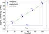 |
Fig. 2 Illustration of the multi-accumulation acquisition mode MACC(ng, nf, nd) with ng = 4, nf = 16, nd = 4 and one reset frame. The integration time tint and exposure time texp defined in Eqs. (1) and (2), respectively, are also indicated. |
2.2 SCS acquisition modes
The H2RG detectors can acquire signal in a so-called multi-accumulation (MACC) acquisition mode (Rauscher et al. 2007) sketched in Fig. 2. The beginning of each exposure is defined by a reset frame. During the reset frame, each pixel is reset in single pixel reset mode or sequentially one by one. Immediately after reset, electric charge accumulates in each pixel as generated by the incident photons. Frames following the reset frame are read frames. During a read frame, each pixel is read non-destructively.
A frame is the unit of data that results from sequentially clocking through and reading out a square area of 2048 × 2048 pixels. Some of the frames may be dropped3 while the integration of signal continues. At the end of the exposure, the signal per pixel is composed of ng equally spaced groups. Each group contains nf consecutive frames sampled up-the-ramp (UTR) and the groups are separated by nd dropped frames. This non-destructive acquisition with UTR sampled data allows for a more precise signal estimate and for the detection of anomalies that can occur during signal integration, such as cosmic ray hits, electronic jumps or deviations from linearity.
The reset after each exposure is performed pixel by pixel in parallel in the 32 output channels. The time needed to reset all the pixels is equal to the time to read the entire detector. This reset scheme reduces as much as possible the transient effect on the first read.
The NISP instrument during nominal observations of the sky acquires data in two predefined acquisition modes (Euclid Collaboration: Jahnke 2025):
The spectroscopic mode with 15 groups of 16 averaged frames and 11 dropped frames between each of two groups, MACC(15,16,11), with the total exposure time of about 574.4 s.
The photometric mode with 4 groups of 16 averaged frames and 4 dropped frames between each of two groups, MACC(4,16,4), with the total exposure time of about 112 s.
This choice was a compromise between the signal-to-noise ratio (S/N) performance that varies depending on MACC schemes (Kubik et al. 2015), the limitations of the on board computational resources, and of bandwidth allocation to downlink the data to ground. It is not planned to vary the acquisition mode depending on the brightness of the observed sources, but specific acquisition modes are implemented for in-flight calibrations, diagnostics, or for sanity checks of the detectors.
Table 1 summarises the main characteristics of the NISP acquisition modes for which detector performances are measured and presented in this paper. The integration time
![Mathematical equation: $\[t_{\mathrm{int}}=\left(n_{\mathrm{f}}+n_{\mathrm{d}}\right)(n_{\mathrm{g}}-1) t_{\mathrm{fr}},\]$](/articles/aa/full_html/2026/03/aa55777-25/aa55777-25-eq1.png) (1)
(1)
relevant for science, and total exposure time
![Mathematical equation: $\[t_{\exp }=\left[n_{\mathrm{f}} n_{\mathrm{g}}+n_{\mathrm{d}}(n_{\mathrm{g}}-1)+n_{\mathrm{r}}\right] t_{\mathrm{fr}},\]$](/articles/aa/full_html/2026/03/aa55777-25/aa55777-25-eq2.png) (2)
(2)
relevant for observation planning, are also reported. The exposure time includes the time of nr = 1 reset frames at the beginning of each exposure. In the table we also give the number of frames n for up-the-ramp UTR(n) acquisition with integration time equivalent to the given MACC, or explicitly n = nd(ng − 1) + nfng.
NISP acquisition modes, MACC(ng, nf, nd), and corresponding UTR(n) used during ground characterisations with n = nfng + nd(ng − 1).
2.3 Removal of common modes using reference pixels
The sensitivity of integrating infrared detectors is limited by dark current and electronic readout noise. The dark current can be lowered down below the natural background level, such as zodiacal light described in Euclid Collaboration: Scaramella (2022), in the high-quality HgCdTe detectors by cooling them to temperatures below 100 K. Then the sensitivity of the array is essentially limited by the readout noise. This read noise is basically the noise of the SIDECAR ASIC and the noise of the Field-Effect Transistors (FET) used as a source-follower employed in the charge-to-voltage conversion in each pixel or “unit cell”, including not only the statistical noise of this FET, but also any noise associated with bias supplies and clocks. While the statistical noise of each unit cell FET is independent, any noise arising from common FETs in the signal chain or from common biases and clocks should be in general correlated.
The reference pixels provided within the detector allow us to reduce this common mode noise at least partially. Reference pixels do not respond to light but contain a simple capacitor Cpix with capacitance similar to that of the active pixels, which is connected to the polarisation voltage of the detector substrate. They are designed to electronically mimic a photosensitive pixel, therefore they are important for tracking polarisation and temperature changes during long exposures (Moseley et al. 2010; Rauscher et al. 2017).
Each of the detector channels has four rows of reference pixels at the top and at the bottom of the array, as presented in Fig. 3. Additionally, the two outside channels include four columns of reference pixels at the outer edges of the array providing a reference for the output at the beginning and at the end of each 2040-pixel row (left and right references).
Various possible corrections using reference pixels were defined and tested in Kubik et al. (2014). Possibilities included using only top and bottom references, using left and right references, or a combination of both. The impact of interpolation between top-to-bottom and left-to-right references and the use of sliding averages in the reading direction for side pixels was also examined. An indicator of the optimal correction was the minimum correlated double sampling4 (CDS) noise level, as it is the easiest noise to measure and is the most sensitive to common modes.
The analysis showed that the optimal correction was to subtract, for each frame, the average of top and bottom reference pixels per output channel to minimise the channel-to-channel noise variations and temporal fluctuations with periods of several frames. The references on the left and right remove common modes on timescales of the readout of one line, suggesting the use of a sliding average centred on the selected line with 4 to 5 pixels on the sides. The effect of interpolation was found to be negligible when optimising noise in photometric and spectrometric exposures. For the ground characterisation and for the flight operations the optimal correction was used, corresponding to ![Mathematical equation: $\[c_{3 m n}^{(c h)}(x, y)\]$](/articles/aa/full_html/2026/03/aa55777-25/aa55777-25-eq3.png) defined in Eq. (2) in Kubik et al. (2014). We recall this correction:
defined in Eq. (2) in Kubik et al. (2014). We recall this correction:
![Mathematical equation: $\[c_{\mathrm{y}}^{(\mathrm{ch})}(m)=\frac{1}{2}\left(\mathrm{T}^{(\mathrm{ch})}+\mathrm{B}^{(\mathrm{ch})}\right)+\frac{1}{2}\left(\mathrm{L}_{\mathrm{y}}(m)+\mathrm{R}_{\mathrm{y}}(m)\right).\]$](/articles/aa/full_html/2026/03/aa55777-25/aa55777-25-eq4.png) (3)
(3)
This equation indicates that for a pixel located in column x ∈ [0, 64[ and in line y ∈ [4, 2044[ in the output channel o ∈ [0, 32[, the correction value ![Mathematical equation: $\[c_{\mathrm{y}}^{\text {(ch)}}(m)\]$](/articles/aa/full_html/2026/03/aa55777-25/aa55777-25-eq5.png) is calculated as the average of all top T(ch) and bottom B(ch) reference pixels in the same output channel ch and the average of the left Ly(m) and right Ry(m) reference pixels located in the window centred on line y and of width 2m + 1.
is calculated as the average of all top T(ch) and bottom B(ch) reference pixels in the same output channel ch and the average of the left Ly(m) and right Ry(m) reference pixels located in the window centred on line y and of width 2m + 1.
The impact of the reference pixel correction on the noise performance is shown in Sect. 5.7.
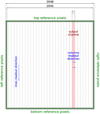 |
Fig. 3 H2RG frame geometry definition with reference pixels on the edges of the array in the 32-output channel mode. The read directions are indicated by the blue arrows. The widths are not in scale. |
2.4 NISP onboard signal estimator
One of the main aspects from the point of view of evaluating detector performance and defining methods for their calibration and correction is that the operation of NISP requires two different exposure times and acquisition modes in order to obtain the best S/N for the targeted scientific objects. The limited daily bandwidth offered by the spacecraft requires sending only the slope calculated on board from data points sampled up the ramp and the associated quality factor (QF) of the fit (Bonoli et al. 2016; Medinaceli et al. 2020).
The NISP signal estimator, denoted hereafter as SNISP, and QF computed on board is based on a likelihood estimator built on the group differences (Kubik et al. 2016). The choice of this estimator was driven by two facts. First, it is a more efficient estimator than the commonly used least square fit, i.e. its variance is lower. This translates directly to a higher S/N, a vital parameter for the scientific outcome of the mission. Secondly, the QF can be computed at the same time as the signal without the need to reprocess the data. This accelerates the computations and minimises the power consumption. The QF allows monitoring the quality of the signal estimate and the linearity of the pixel response, which otherwise would be impossible to track in the presence of non-destructive readout and signal fitted on board.
3 Ground characterisation campaigns
This section describes the objectives, workflow and tools developed for the characterisation campaign of the Euclid infrared detectors. We provide a detailed description and motivation of the testing process, and we describe the software developed for the data acquisition and verification in near real-time.
3.1 Objectives
The production of flight parts is a lengthy process that begins with acceptance tests and the associated requirements. The SCS triplets and their individual components (SCA and SCE) have undergone extensive testing throughout the production process. This includes acceptance testing and ranking at the Detector Characterisation Laboratory (DCL) at NASA/GSFC (Waczynski et al. 2016; Bai et al. 2018), SCE testing at NASA Jet Propulsion Lab (JPL, Holmes et al. 2022), individual component tests of the SCAs at the CNRS-IN2P3 Center for Particle Physics in Marseille (CPPM), and thermal vacuum (TV) tests of the FPA in its final configuration at the CNRS-INSU Laboratory of Astrophysics in Marseille (LAM) facility. The ground characterisation was carried out in three stages:
Acceptance tests at NASA allowed the selection of the best 20 detectors from a set of 60 that were available for Euclid and provided overall average reference of the dark current, readout noise, and QE for subsequent detailed characterisation and performance measurements,
characterisation tests at CPPM provided per-pixel performance of individual detectors taken in a cross-validated and controlled environment, and
tests of all detectors integrated onto the FPA of the NISP instrument.
A complete overview of characterisation campaigns carried out by the NISP detector team can be found in Barbier et al. (2018).
The goals of the ground characterisation campaigns were to
tune the operating parameters (such as the polarisation voltage, the gain, or the baseline) for all the detectors to optimise their performance;
produce detailed pixel maps of detector performance for use by the science ground segment (SGS) as references for flight calibrations;
produce readout chain correction functions with a relative accuracy of 1%;
estimate the accuracy of the in-flight calibration procedure of the readout chain through tests mimicking flight conditions;
create models of how detector properties and performance are modified under varying environments experienced during flight, in order to monitor and quantify their impact on the detector chain error compared to optimal performance determined in ground tests;
study the behaviour of the flight detectors in order to anticipate their evolution and the degradation of their performance during the mission.
Handling the large volumes of data generated during these tests, which can reach up to 0.5 TB per day per SCS, is crucial. Ensuring stability and reproducibility throughout the testing process is also essential. This requires a well-controlled and continuously monitored cryogenic environment, along with careful management of both the optical and the electrical equipments.
This paper focuses on the first and second goals and it presents the performance of flight detectors in their final configuration. Therefore most of the results presented in this paper are derived from the TV (thermal vacuum test) dataset. Only the QE (Sect. 5.5) and interpixel capacitance (IPC, see Sect. 5.4) maps were derived from tests at DCL and CPPM tests respectively.
The pixel effects reported in the sections below impact the signal measurements and introduce systematic errors. Based on these measurements, per-pixel correction functions can be derived with a requirement of 1% accuracy on the relative response of the detector chain (Secroun et al. 2016; Barbier et al. 2018). The principal difficulty in the detector chain response calibration is to fulfil the correction at 1% accuracy over the full dynamic of the detector. This translates into a compliance to the test specifications ranging from very low dark signal and zodiacal background to the highest calibration fluence, knowing that most of the fluence (total integrated signal) of the sources of interest will lay in the range of a few thousands of electrons per pixel.
3.2 Set-up
The Euclid Consortium used two facilities to carry out the detectors’ characterisation. Firstly, the CPPM benches (Euclid Collaboration: Secroun et al., in prep.) have been specifically designed to meet the needs of pixel-by-pixel characterisation of the NISP detectors’ performance, taking into account the 1% accuracy objective. Significant effort has therefore been devoted to minimising and controlling the systematic errors introduced by the benches themselves. In summary, two twin cryostats (to ensure redundancy) can each accommodate two detectors being read in parallel, using Markury electronics (see Sect. 4.4). These cryostats consist of an outer stainless steel vessel that maintains the vacuum, an internal copper layer coupled to a 90 W cryocooler that ensures cooling within the cryostat and at the focal plane, and a second internal aluminium layer that simultaneously provides a deep dark environment and a very homogeneous flat field (Euclid Collaboration: Secroun et al., in prep.). The detectors’ temperature can be controlled with a precision better than 10 mK and a stability of 1 mK. The flux exhibits homogeneity better than 1% across the detector and a flux stability well below 1% (Euclid Collaboration: Secroun et al., in prep.). These benches enable measurements of detector performance dependencies on temperature (typically between 70 K and 120 K), wavelength (across the entire sensitivity range of the detectors), and flux (from dark level to several times saturation).
Secondly, the ERIOS space simulation chamber at LAM (Costille et al. 2016) has been designed to test full instruments like NISP. This chamber, measuring 4 m in diameter and 6 m in length, maintains a secondary vacuum (~10−6 mbar) and a cold ambient environment throughout its entire chamber (45 m3) at a temperature close to that of liquid nitrogen. To ensure mechanical stability, and hence accurate measurements, the instrument’s supporting table is connected to a 100tone concrete block under the floor and rests on pillars via spring boxes. The Thermal and Mechanical Ground Support Equipment (TMVS) developed for NISP TV provide thermal and mechanical interfaces of the instrument and simulate the PLM thermal environment with a stability of 4 mK.
3.3 TV test flow
The characterisation workflow, or test flow, is designed to produce high-quality data from the flight SCS within a time frame compatible with the NISP testing schedule. Data is collected continuously, 24 hours a day, over a 14-day period, with 3 days specifically allocated for tuning of the SCS system parameters. The definition of the test flow is the result of a trade-off between various constraints and requirements. Key considerations while defining the test flow include
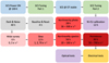 |
Fig. 4 TV workflow as implemented and executed during the 14-day testing period. In the boxes we specify the type of test, the test duration in hours, and the range of fluxes that were used. No indication of flux values means that the test was performed in dark conditions. All tests were performed with a 99.73% time efficiency. |
Schedule management: Ensuring the schedule remains on track with built-in margins to accommodate potential set-up failures.
Thermal stability: Minimising the number of cooling cycles and large temperature variations across different tests.
Mitigating long exposure issues: Avoiding long test runs that might be affected by spurious exposures.
Latency mitigation: Controlling latency effects by ordering tests based on increasing levels of illumination.
Detector maps obtained during acceptance tests are used as cross-references. While these maps are not intended for direct verification or validation, they help ensure data coherence between different test facilities. The test flow, presented in Fig. 4, includes the following runs,
system temperature stabilisation,
SCE register tuning,
near-infrared calibration unit (NI-CU; Euclid Collaboration: Hormuth 2025) calibration and validation (stability and accuracy),
baseline and reset noise measurements,
dark measurements (includes the measurement of single frame readout noise and the slope noise),
non-linearity measurements,
latency measurements, and
additional optical and electrical tests.
3.4 Data acquisition software
The measurement of any detector characteristic is defined as a coherent entity consisting of pre-programmed acquisition cycles and environmental configurations. The number of cycles is typically determined by the required measurement accuracy, and their order is based on the physics of the detector and the specific parameters being measured. These measurements must be performed according to a predefined scenario that ensures the stability of the environmental conditions. This is crucial for meeting the statistical requirements necessary for the characterisation of individual pixels and mitigate contamination from persistence signal between exposures.
The runs specified in the test flow are executed by the data acquisition software (DAS). The scheme of the runs executed automatically according to the test plan is shown in Fig. 5. The building block of each run is an exposure. It consists of a ramp of non-destructive reads and the accompanying environmental settings, including SCS (gains, bias voltages) and NI-CU settings (e.g., LED selection and its current and duty cycle). The set-up providing illumination is described in detail in Euclid Collaboration: Hormuth (2025).
The CPU time is used to synchronise the environment and illumination settings with the SCS readouts with a precision better than 0.5 seconds. The lighting set-up is controlled by the DAS, which triggers key events such as switching the LEDs on and off. For ground characterisation, up-the-ramp acquisitions UTR(n) were used with the number of frames n equivalent to the specified MACC (Table 1). The frames corresponding to the MACC readout were selected, if needed, during the post-acquisition analysis of data.
The overall workflow is managed by a super scheduler, i.e. pseudocode of specifications, that generates a scenario of the test flow covering the 14 days of TV tests. The scheduler supports asynchronous tasks (Williams et al. 2019), which is one of the most difficult aspects of implementation.
Thanks to the automated data acquisition system, the tests were conducted continuously, 24 hours a day, achieving a time efficiency of 99.73%. This indicates that less than 0.3% of the total time was lost due to failures.
 |
Fig. 5 Hierarchical data structure defined for the SCS characterisation campaign. |
3.5 Data quality quick check
The data quality during acquisition is monitored by comparing the CDS signal and noise levels with approved reference values. Statistical analysis performed at the level of individual rows, columns, channels, or frames allows for verification of both temporal and spatial characteristics of data, and generates alerts in case of anomalies. The system, based on alerts, verifies data in less than one hour after a two-day acquisition period.
4 Detector configuration settings
The performance of pixel sensors involves a delicate trade-off between noise characteristics and the accessible dynamic. For photometric applications, a minimum dynamic of 60 ke− is required and there is a requirement on the maximum acceptable readout noise value of 13 and 9 electrons in photometric and spectroscopic acquisition modes respectively (see also Sect. 5.7).
The accessible dynamic of the signal is primarily determined by the gain of the SCE and is constrained by several factors, including the non-linearity of the SCE at both the upper and lower limits, the inhomogeneity of the baseline and the minimum pixel full well capacity which is defined by the applied polarisation voltage. On the other hand, both the position of the baseline, the polarisation, and the SCE gain impact the detector noise performance.
4.1 Baseline settings
First, the level of the baseline in the 65 535 counts range of the 16 bits ADC is of course a direct driver of the maximal science signal achievable in both acquisition modes. The limiting factor to the lowering of the baseline is the low end of the differential non-linearity (DNLlow) of the ADC, which is on the order of 1000 ADU. If the baseline is set at the lowest possible level not exceeding the lower (DNLlow) threshold, good stability is obtained for dark current and for weak signals, but with readout noise slightly higher than in the middle of the ADC’s dynamic. We therefore set the baseline 5000 ADU higher than the lower (DNLlow) limit allows, in order to minimise the readout noise while maintaining sufficient dynamic for scientific signals.
4.2 Detector polarisation voltage settings
The detector polarisation voltage, which is the difference in voltage between the backside substrate and the diode reset voltage, was set to 500 mV. This value was found to be a good compromise between noise performance, the dark current value and full well capacity. The compromise was based on the following considerations: firstly, setting the highest possible polarisation, while keeping the 95th percentile of total noise below specification; secondly, achieving a maximum useful integrated signal of 60 ke− in photometric acquisition mode; and thirdly, shifting the full well capacity (130 ke−) above the ADC saturation (65535 ADU) to minimise diode non-linearity.
4.3 SCE gain settings
Various preamplifier gains5 were tested and discussed during the non-recurring engineering (NRE) phase6 and acceptance tests. Advantages and disadvantages were raised for three possible preamplifier gain values, 15 dB, 18 dB and 21 dB, consistent with the target S/N. The final choice was to use the lowest SCE gain of 15 dB to improve the dynamic from 60 ke− to 115 ke−, still below the ADC saturation. This mitigates the non-linear effects close to pixel full well and increases the range of the measurable signal, which is very important when calculating the persistence contribution for subsequent exposures.
4.4 Tuning of flight SCS parameters
To speed up the tuning process of the 16 SCSs and of the SIDECAR ASICs, the data acquisition is done in parallel, but some parameters are adjusted one by one within a certain predefined range, already optimised during the acceptance tests carried out by NASA with the expertise and supervision of Markury Scientific7. At the end, after optimising the different functions, each SCS has its own set of parameters. The tuning was carried out in the following steps.
Firstly, the dynamic response of the pixels was optimised by analysing the unit cell current controlled by the ROIC voltage settings. The minimised value in this case is the residual signal that can be observed on the first pixel adjacent to the stimulated pixel with respect to the reading direction, if the cell current is too weak to drive the signal within a time slot of one clock (10 μs). Obviously, this current must be kept as low as possible to reduce the power consumption of the ROIC during the readout sequence.
Secondly, the CDS noise of the groups taken from the MACC(4,16,4) photometric acquisition mode, which represents the most demanding scenario in terms of noise performance, was minimised. The values of median noise in each of the 32 channels and the value of the noisiest channel were used as the references for this process.
Thirdly, baseline adjustment was performed through the reference voltage of the capacitive trans-impedance preamplifier before the 15 dB gain setting. For each detector, a maximum value was selected from the 32 DNL limits measured during the acceptance test for each output channel and used as the lowest threshold for the median baseline of the reference pixels. The baseline setting is driven by the reference pixels, because they exhibit lower baseline values compared to the photosensitive pixels and too low baseline of reference pixels could introduce non-linearities in the signal during reference pixel correction. A closed-loop algorithm was developed to rapidly converge to the target baseline values by adjusting the bias for the 16 SCS in parallel. At the end of the tuning process, the average dynamic of each SCS is around 115 ke−.
5 Pre-launch SCS properties and performance
This section is the core section of the paper. Here, we present the main properties of the Euclid near-infrared detectors as measured during the ground characterisation campaign. For each property, we describe its physical background and its role in the overall performance of the detector system. We then outline the measurement protocols used to evaluate each property, presenting the steps taken to ensure accuracy and consistency. Finally, we present the measurement results, highlighting their potential implications for detector performance.
In the sections below, we identify the detectors either by their position in the focal plane (e.g., DET 11) or by their SCA serial number (a five-digit identifier in the form 18***). The table below provides the explicit correspondence between these two naming conventions:
| FPA position | 41 | 42 | 43 | 44 |
| SCA number | 18 458 | 18 249 | 18 221 | 18 628 |
| FPA position | 31 | 32 | 33 | 34 |
| SCA number | 18 280 | 18 284 | 18 278 | 18 269 |
| FPA position | 21 | 22 | 23 | 24 |
| SCA number | 18 268 | 18 285 | 18 548 | 18 452 |
| FPA position | 11 | 12 | 13 | 14 |
| SCA number | 18 453 | 18 272 | 18 632 | 18 267 |
5.1 Disconnected pixels
Pixels with missing or not fully connected indium bumps between the p-on-n diode and the metal pad of the ROIC occur infrequently and are an issue in the detector system that needs to be characterised. These pixels are permanently inoperable. To efficiently discriminate between disconnected and operational pixels, a strategy was adopted to examine the pixel output response to substrate bias (Dsub) at room temperature.
Connectivity tests were performed before the entire set-up was cooled down. Two sequences of 64 ramps were acquired in UTR(1) with Dsub set to 500 mV and 550 mV, respectively. The estimator used to identify the disconnected pixels is the difference between the pixel response measurements b1 and b2 at two different polarisation values (changing Dsub) of the substrate. Specifically, the estimator is calculated as
![Mathematical equation: $\[d=\frac{b_2-b_1}{\left\langle b_2-b_1\right\rangle}-1,\]$](/articles/aa/full_html/2026/03/aa55777-25/aa55777-25-eq6.png)
where ⟨b2 − b1⟩ is the spatial mean of the difference of two images b1 and b2. For operating pixels, this value is close to 0, whereas for disconnected pixels it is −1. In practice, a threshold of −0.7 was set to discriminate between connected and disconnected pixels. Pixels with estimator values ranging from −0.7 to −0.2 were considered potentially disconnected and were recorded for further investigation.
Depending on the SCA, the number of disconnected pixels ranges from a few hundred to a few thousand. The precise numbers for each detector are reported in Table A.1. The results show that disconnected pixels are randomly distributed, with no noticeable clusters. Reference pixels formally have a disconnectivity estimator d close to −1 due to their capacitive behaviour, but should not be considered inoperable. The temporal stability of disconnected pixels was tested in three independent tests, at DCL, at CPPM and at LAM, in part with different bias voltages. The two populations of pixels, connected and disconnected, were shown to be stable over time and thermal cycling.
5.2 Baseline and dynamical range
Since in-flight acquisitions are based on MACC ramps, the baseline is defined as the average value of the first 16 frames after a pixel reset taken in dark conditions. It represents the pedestal value for sampling up the ramp. The tuning of the baseline value, described in Sect. 4, is critical since it defines the maximal signal that can be detected, and it prevents entering into the non-linear zone of ADC if the baseline setting is correct.
The ‘master’ baseline B is measured as the average baseline over 500 ramps of 16 frames. For Euclid H2RG detectors, the baseline typically ranges from 7000 to 15 000 ADU before reference pixel subtraction, as shown in the baseline image in Fig. 6, and is reduced to 4000 to 10 000 ADU after reference pixel correction as indicated in Fig. 7. Table A.1 reports the median baseline values of science pixels after reference pixel correction. Additionally, the median baseline values of reference pixels are provided for each detector.
For photosensitive pixels, the difference between the 5th and 95th percentiles (spatially over an array) of the baseline values is about 7000 ADU and this spread remains unchanged by the reference pixel correction. The shape of the distribution of baseline values per detector deviates significantly from a typical Gaussian function, which may be related to the manufacturing process.
The baseline of the reference pixels differs significantly from that of the photosensitive pixels; it is lower and more uniform than the one of photosensitive pixels. For reference pixels, the per detector median baseline values, with the settings described in Sect. 4, range from about 5000–6000 ADU. The difference between the 5th and 95th percentiles is slightly less than 3000 ADU.
The value of the baseline is directly related to the dynamic of the pixels of 115 ke−, which corresponds to a flux of 1000 e− s−1 in MACC(4,16,4) and 200 e− s−1 in MACC(15,16,11). The spatial spread of the baseline values also represents the spatial spread of the pixel dynamic. It means that not all pixels will be able to observe an equally strong signal, some will saturate earlier or, on the other hand, the same signal falling on pixels with different baseline values will be subjected to different sources of non-linear behaviour.
Photosensitive pixels with a baseline significantly higher than 60 kADU do not have sufficient dynamic for scientific applications and should be considered as unusable. Pixels with baseline values lower than the acceptable DNL range shall be also be flagged as unusable. These pixels are included in the bad pixel budget described in Sect. 5.3.
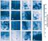 |
Fig. 6 Baseline image of the whole FPA before reference pixel correction. This and all subsequent detector maps are displayed in the R-MOSAIC coordinate system (Euclid Collaboration: Jahnke 2025). |
5.3 Bad pixels
The survey efficiency requirement translates into a 95th percentile requirement of operational pixels for science. Pixels can be inoperable permanently or for some amount of time, for example if they are saturated by an energetic particle hit and the signal cannot be recovered. Pixels are considered permanently inoperable or ‘bad’ if they meet any of the following criteria:
Pixels that are disconnected from the circuit are non-functional for obvious reasons.
Pixels that have the QE of less than 1% are non-functional due to lack of light response.
Pixels whose baseline values are outside the acceptable DNL limits (B < DNLlow) are non-functional, as they may exhibit non-linear behaviour that is difficult to correct.
Pixels with B > 60 kADU are non-functional because they lack sufficient dynamic for scientific purposes.
The budget of the inoperable pixels in each of the above-mentioned categories, as well as their combined total, excluding double-counting, is shown in Table 2. The number of nonoperational pixels does not exceed 0.2% per detector, which is far below the requirement. The spatial distribution of bad pixels is typically sparse across the detector, as illustrated in Fig. 8. Clustering is observed only in pixels with low QE.
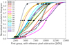 |
Fig. 7 Distribution of the baseline values after reference pixel correction. The black dots represent the 5th, 50th, and 95th percentiles of the science pixels baseline distribution. |
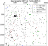 |
Fig. 8 Example of the spatial distribution of bad pixels across an array. |
5.4 Interpixel capacitance
In the infrared pixel detectors with the source follower per detector input stage, which are based on CMOS hybrid readout technology, there is a phenomenon known as electrostatic cross-talk between pixels. This is because the fields coming from the edges of the node capacitors in neighbouring pixels affect the voltage readings in the central pixel. This results in a dependence of the signal in the central pixel on the charges in adjacent pixels. This effect is typically modelled by introducing a coupling capacitance between pixels, effectively connecting every pixel to its neighbours. Naturally, the IPC is becoming more important in near-infrared detectors as pixel size decreases (Moore et al. 2004, 2006; Fox et al. 2009). It is crucial to understand that this IPC is not the same as charge diffusion. The latter involves the physical movement of charge carriers between neighbouring pixels before charge collection and is a stochastic process. Signal noise resulting from charge diffusion in neighbouring pixels is uncorrelated. IPC cross-talk occurs after charge collection and is deterministic, resulting in correlated signal noise in neighbouring pixels.
The presence of IPC needs to be accounted for in applications like photometry or astrometry, as it blurs the PSF, modifying both the size and shape of the sources. Moreover, as it correlates the Poisson noise of the signal in adjacent pixels, it can lead to an overestimation of the gain (ADU/e−), measured using photon-transfer-curve, as described in Sect. 5.6, and consequently to an overestimation of the QE while lowering the effective S/N in each pixel (Moore et al. 2006; Fox et al. 2009).
Furthermore, pixels frequently display a non-linear response, as the pixel capacitance depends on the charge. This deviation from the nominal capacitance value is typically modelled separately, leaving the IPC to be treated as a linear effect. However, accounting for IPC is essential, particularly when calculating the conversion gain of the system (Secroun et al. 2018; Le Graët et al. 2022, 2024).
The IPC for the Euclid SCAs was measured using the single-pixel reset (SPR) technique enabled by the guide mode8 of H2RGs. SPR enables the direct characterisation of IPC, eliminating the necessity for an illumination source. This SPR characterisation mode is incorporated into the command structure of the Euclid firmware and can be used as part of on orbit calibration. This method is useful for isolating IPC, since the charge is not generated in the photosensitive material, and is therefore not susceptible to the effects of charge diffusion (Finger et al. 2006; Dudik et al. 2012). In SPR, following the setting of all pixels in the SCA to a single voltage and the initial readout, a grid of widely spaced single pixels is reset to a second voltage level. Following this reset, all pixels are again read out. The difference of these two images will reveal any IPC as a signal in pixels adjacent to the reseted pixels. The 3 × 3 pixel IPC kernels were obtained for all SCA through SPR testing. These couplings are uniform across the detector arrays, with the observed dispersion of order of 1% if the specific regions called ‘voids’ are excluded. The ‘void’ regions, presumably with a missing epoxy layer between the HgCdTe substrate and the ROIC, exhibit a significant deviation from the average value (yellow regions in Fig. 9) and affect the uniformity of the detector response, but the flat field correction can remove this effect.
To achieve an accuracy below 1% for the central pixel, we provide in Fig. 10 the average IPC value per detector. The parasitic coupling introduced by IPC contributes to less than 3% of the pixel’s node capacitance and produces less than 1% of cross-talk between nearest neighbours. The median values of the IPC kernel are reported in Table A.1.
Bad pixel budget per detector as measured during ground tests. In the last row the combined total, excluding double-counting, is given.
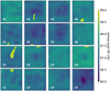 |
Fig. 9 Map of the central pixel value of the IPC kernel. The void regions are visible as yellow shapes. |
5.5 Quantum efficiency
Quantum efficiency is a measure of the fraction of photons incident on a detector that are converted into electrons and detected as a signal. A high QE is therefore essential for a sensitive and efficient detection system. By its nature, QE depends on the incident photons’ wavelength. Measuring QE generally involves comparing the signal recorded by a characterised sensor with the signal recorded by an independent calibrated signal sensor (such as a photodiode). The measurement is also sensitive to the efficiency of charge collection in the detector and to the effective charge-to-voltage conversion.
For the NISP detectors, QE data were obtained at DCL during acceptance tests. The DCL dataset includes pixel QE maps measured at 40 different wavelengths ranging from 0.6 to 2.6 μm, with a resolution of 50 nm steps and an absolute accuracy of the QE measurements of 5%. A map of the mean QE in the NISP JE band, calculated as the average QE from eight measurements in the wavelength range of (1168–1567 nm), is shown in Fig. 11. The reported median QE values are above 90% and the 95% of pixels have QE above 80% across the entire spectral range of Euclid as shown in Fig. 12. Additionally, we provide the explicit values for the 5th, 50th, and 95th percentiles of the average QE in the NISP photometric bands YE, JE and HE. in Table 3. For the QE measurements, a detector-averaged gain, calibrated with a dedicated electronic board was used. This may account for QE values exceeding 100%. Additional factors affecting the measurement precision include the relative accuracy of the photodiode calibration, the uniformity of the illumination, and the pixel area.
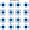 |
Fig. 10 Mean IPC kernel per detector with sub-percent accuracy. |
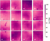 |
Fig. 11 Map of the average QE in the NISP JE band (1168–1567 nm). |
5.6 Conversion gain
The conversion gain is essential for measuring a variety of detector properties, including readout noise, dark current, and QE. Since it defines the relationship between digitised counts from the ADC and the photogenerated electrons detected by the system, it allows for accurate calculations of detector performance parameters in physical units.
The gain is generally viewed as a combination of three distinct processes: (1) Charge-to-voltage conversion from electrons to volts in the photodiode, (2) voltage amplification and buffering in the ROIC, and (3) conversion from volts to ADU in the external electronics. A detailed description of these transfer functions can be found in Barbier et al. (2018). A common method for determining the conversion gain is the mean-variance method, also known as the photon transfer curve (PTC) described in Janesick (2007). In this approach, a series of exposures with varying fluences are taken under constant flux to generate data. The signal variance is plotted against the mean signal of each exposure, and a linear fit is applied to this data. The inverse slope of this line represents the total conversion gain from ADU to electrons.
The mean-variance curves were constructed using 15 flat-field acquisitions, where the variance and mean signal were computed for each pixel across 15 ramps taken under the same flux conditions. Next, the average spatial variance was calculated for each of the 32 readout channels of 64× 2040 pixels after baseline subtraction, which removes fixed pattern noise and excludes bad pixels. Spatial correlations between pixels were neglected. Spatial dispersion in the gain predominantly arises from the output buffer of the multiplexer (MUX), the channel amplifier before the ADC and the ADC itself – all these contributions are shared across the same readout channel. Per-pixel contributions, such as the pixel source follower gain and transimpedance gain (charge-to-voltage conversion factor), are not included, as it is an average spatial variance per channel. Average conversion gain values for each channel are computed and shown in Fig. 13. The dispersion of the conversion gain per channel is less than 1%. In Table A.1 the average values of conversion gain per detector are reported. The average conversion gain of the focal plane array (FPA) is 0.52 ADU/e−, with about 3% variation between different arrays. Average conversion gain values for each channel are used to convert ADU to electrons in subsequent analyses.
The influence of the dynamic used to compute the conversion gain was studied in Secroun et al. (2018). A method for evaluating gain with higher spatial resolution, using 16 × 16 super-pixels, was derived in Le Graët et al. (2024). Using the conversion gain measured per super-pixel, the effect of gain and QE can be decorrelated, thus obtaining a more precise measurement of QE. Le Graët et al. (2024) also discusses the influence of IPC and signal non-linearity and proposes a method for estimating gain corrected for these factors.
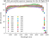 |
Fig. 12 QE as a function of wavelength. The points indicate the lowest 5th percentile per detector. 95% of the pixels have QE values higher than 80% over most of the wavelength range. |
Percentiles (5th, 50th, and 95th) of the average QE in the NISP photometric bands YE, JE, and HE.
5.7 Noise performance
The source of noise can be the signal source itself, but in the absence of illumination, the dominant sources of noise are in the readout electronics and in the resistive component of the light-sensitive material. The resulting noise is called readout noise. It describes the typical variability of recorded counts from one reading to another in the absence of illumination and, in the case of sky observations, adds to the noise from the source itself. Which noise sources are dominant in a given case depends on the exposure time, acquisition mode, and signal estimation method. Reset noise is the noise of the pixel’s zero level generated by the diodes when connecting to the power supply. It is also called kTC noise, as it varies proportionally with temperature T and pixel capacitance C along with the Boltzmann’s constant kB as the proportionality factor. Fortunately, the reset noise is completely removed by sampling up-the-ramp, but it is interesting to quantify it to see by how much the offset of signal integration can vary from exposure to exposure. It is also a reference for checking the state of the detectors. The comparison of the current measured baseline and the reference baseline should be consistent with the kTC noise.
In the case of very bright sources, which saturate the detector in a very short time, a typical solution is to use the CDS technique, which makes it possible to easily adapt the exposure time while avoiding saturation, thus increasing the accuracy of the measurement. In such a case, it is necessary to estimate the readout noise of a single readout. In the case of Euclid, the acquisition mode is MACC rather than CDS, and no change in exposure time is anticipated for bright sources. However, the noise value of a single readout is required as input for the algorithm of signal estimation using multiple frames up-the-ramp (Kubik et al. 2016). Finally, the noise characteristics will also depend on how the flux is estimated from up-the-ramp samples.
The following sections present an overview of the noise characteristics of the Euclid H2RG detectors. First, typical reset noise values are discussed, followed by an overview of single frame readout noise and finally the readout noise of the signal estimator, when multiple signal readouts are taken up the ramp and the slope is calculated using the algorithm described in Kubik et al. (2016), is presented.
5.7.1 Reset noise
To estimate the reset noise of the NISP detectors, 500 dark exposures of 16 frames up-the-ramp were taken. The 16 frames were averaged per pixel for each of the exposures, forming 500 groups. The standard deviation of the groups per pixel was computed and this represents the reset noise of the first group in each of the science acquisition modes of NISP detectors. These calculations were performed twice: first prior to the reference pixel correction, and then after the frames were corrected using reference pixels. In Fig. 14 we show the obtained values as well as the reset noise of reference pixels.
For photosensitive pixels, the reset noise is typically in the range of 25 ADU rms (about 50 e− rms), while reference pixels have a reset noise of around 20 ADU. The noise is fairly homogeneous within each of the 32 channels of a detector, but each channel has a different average noise level. The reference pixel correction effectively reduces the baseline noise of photosensitive pixels to approximately 23 ADU and reduces the spatial dispersion of noise levels across channels. The FPA average reset noise before reference pixel correction is equal to 25.5 ADU with a 3.5% dispersion between arrays. After reference pixel correction, the average FPA reset noise is reduced to 23.9 ADU and the dispersion between detectors is lowered to 2%. The median values of the reset noise after reference pixel correction are reported in Table A.1. There is a correlation between the reset noise of the reference pixels and the correction amplitude: higher reset noise in the reference pixels results in a stronger correction.
5.7.2 Single frame readout noise
To estimate the detection chain noise of a single readout we used 90 exposures of 394 frames, UTR(394), acquired with no illumination. After reference pixel correction, the non-overlapping consecutive pairs of frames are subtracted to form 197 CDS frames per exposure. The single frame readout noise is computed as the standard deviation per pixel across these 197 CDS frames and divided by ![Mathematical equation: $\[\sqrt{2}\]$](/articles/aa/full_html/2026/03/aa55777-25/aa55777-25-eq7.png) to account for two frames in one CDS pair. The shot noise contribution of the dark current is negligible and is not subtracted. The median per pixel is then taken across 90 values of noise frames to reject glitches and to form the final single frame readout noise map. This map is converted to electrons using the average conversion gain per channel.
to account for two frames in one CDS pair. The shot noise contribution of the dark current is negligible and is not subtracted. The median per pixel is then taken across 90 values of noise frames to reject glitches and to form the final single frame readout noise map. This map is converted to electrons using the average conversion gain per channel.
The values of median noise per detector are reported in Table A.1. The median values of the single frame readout noise of Euclid H2RG detectors are less than 15 e− rms. The noise distribution is log-normal, the 95th percentile does not exceed 16 e− rms and the 5th percentile lies between 10 e− rms and 14 e− rms depending on the SCA as shown in Fig. 15.
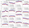 |
Fig. 13 Conversion gain per channel computed using flat-field ramps with increasing (IR3 < IR4 < IR5) illumination levels. In the legends for each detector the average gain over the 32 channels and the dispersion between channels are given. For all the three illuminations the mean conversion gain for the whole FPA is 0.52 ADU/e− with a 3% variation between arrays. The channel-to-channel gain variation inside a detector is less than 1%. The gain variation with signal is described in Le Graët et al. (2024). |
5.7.3 Readout noise
The readout noise (RON) of the detecting system is defined as the standard deviation per pixel of the signal estimates SNISP. It depends on the total exposure time and on the acquisition mode.
To estimate the readout noise in photometric and spectroscopic acquisition modes, the same slopes used for the dark current computation (see next section) were used. The slopes were multiplied by the integration time characteristic for each of the acquisition modes, i.e. by 87.2 s and by 549.6 s, respectively, to obtain the total integrated signal in electrons. After that, the standard deviation per pixel was computed from the signal variation between the 90 available ramps. The median values per detector are reported in Table A.1. The median photometric noise σph is below 7 e− rms. The median spectroscopic noise σsp is below 9 e− rms. The noise does not scale with exposure time, because different acquisition modes are used. In spectroscopic mode 15 groups are taken, effectively lowering the noise in signal estimation compared to when fewer groups would be acquired along the ramp (Kubik et al. 2015).
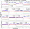 |
Fig. 14 Reset noise of science pixels before (blue circles) and after (red triangles) reference pixel correction. The reset noise of reference pixels is shown as green circles. For each detector in the legend the average reset noise over the 32 channels is indicated, and in parentheses the relative dispersion of the average reset noise between channels is given. At the top (in the title) we indicate the average reset noise over the whole FPA and the dispersion between detectors before reference pixel correction. The values after reference pixel correction are given in brackets. |
5.8 Dark current
Pixel dark current is another major factor affecting the performance of pixel detectors. Its cause is the leakage current of the photodiode, which is mainly thermally generated. However, the measurement is also sensitive to the differential voltage drift between reference and science pixels. Hence, an important factor to consider when assessing the dark current is the whole SCS – comprising the SCA and the SCE components. Moreover, it is recommended to use matching dark and science exposures for most astronomical infrared array detectors to remove any residual bias (Rauscher et al. 2007). This is achieved by ensuring that the dark exposures are taken using the same acquisition mode as the science exposures. This is why in this section we report values of ‘photometric’ and ‘spectrometric’ darks that are evaluated using the MACC(4,16,4) or MACC(15,16,11) acquisition modes, respectively.
At the operating temperature of 87 K, the pixel leakage current of H2RG detectors is very low, typically below 10−3 e− s−1. This is generally good for science, but also makes it difficult to measure with high accuracy in science acquisition mode. Accurate dark current measurements typically require many repeated exposures. For example, assuming a dark current of 10−3 e− s−1 we would need to take more than 7000 ramps (requiring more than a week of dark measurement) to achieve 1% accuracy on the dark in photometric acquisition mode for pixels with the readout noise close to the median value. Therefore, in our measurements, we did not aim for an accuracy of 1% when measuring dark current, but were interested in measuring dark current under ‘operational’ conditions with fixed MACC modes and exposure times.
Dark current values were computed from 90 exposures acquired with UTR(394), each with a total exposure time of about 10 minutes. The reference pixel correction was applied to all exposures as the first step of data reduction. The NISP onboard signal estimation algorithm (see Sect. 2.4) used was the one implemented in the flight electronics on board Euclid to obtain comparable values (Kubik et al. 2016). To calculate the signal among 394 acquired frames, only the frames corresponding to the in flight acquisition modes, i.e. MACC(4, 16, 4) or MACC(15, 16, 11), were selected as input to the algorithm. Thus, two different values of dark current were obtained: ‘photometric’ dark dph and ‘spectrometric’ dark dsp respectively. After removing exposures with detected anomalies at the pixel level, which are very few and usually correspond to electronic glitches, the cosmic rays component is insignificant due to the orientation of the focal plane perpendicular to the Earth’s surface, a median filter was applied to obtain dark current maps.
The average conversion gain per channel was applied to convert ADU to electrons. The results for dark current measurements dph and dsp, given in Table A.1, are expressed in electrons per second, allowing easier comparison between the two. A higher value of dsp compared to dph could be due to the imperfect measurement conditions (e.g. with low-level residual stray-light in the cryostat). Also, a different acquisition mode can affect the measured value of the dark current, but it is difficult to estimate the relative influence of different factors on the measurement. The influence of persistence is excluded, as the detectors were kept in the dark conditions for a long time before the measurement began.
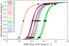 |
Fig. 15 Cumulative distributions of single frame readout noise for the 16 detector arrays after reference pixel correction. The black dots represent the 5th, 50th, and 95th percentiles of the distribution. |
5.9 Non-linearity
The response of H2RG CMOS detectors, like that of many other pixel-based devices, can deviate from the ideal linear behaviour (Vacca et al. 2004; Plazas et al. 2017; Mosby et al. 2020). This analysis concentrates on ‘classical’ non-linearity, namely the non-linearity associated with the conversion from charge to voltage domain. In contrast to CCD devices, the non-linearity in HgCdTe detectors varies from pixel to pixel. Attaining sub-percent accuracy in correcting for this non-linearity is crucial for the mission’s scientific objectives. In this section, we examine the extent to which the pixel response deviates from ideal linear behaviour following the tuning of the electronic registers.
5.9.1 Characterisation of detectors non-linearity
The non-linearity is measured separately in photometric and spectroscopic acquisition modes at several fluence levels ranging from 1000 up to 80 ke− which corresponds to about 60% of the typical pixel full well (assumed here to be of 130 ke− on average). Typically, non-linearity is a measure of how much the signal recorded at a pixel in the maximum dynamic deviates from the signal measured as a linear fit to the start of the ramp of that pixel. The response of the pixel is then modelled by a polynomial function, the inverse of which is used as the linearising function of the measured counts. In the case of Euclid, the inherently non-linear signal sampled up-the-ramp is estimated on board using the NISP onboard signal estimator SNISP described in Sect. 2.4 and the slope result is sent to the ground. SNISP is subject to a systematic error due to the non-linearity of the pixel response, since it assumes a linear behaviour. We therefore need to quantify the deviation of SNISP with respect to the expected linear signal, denoted hereafter as Slin.
To determine the degree of non-linearity in spectroscopic acquisition mode, a typical acquisition pattern involves a sequence of 30 flat-field ramps of UTR(394). The number of exposures per flux is calculated in order to maintain a relative flux error below 1%, provided that the number of exposures does not exceed 30. Beyond this threshold, the measurement was constrained by time limitations. The ramps after reference pixel correction are modelled one by one using a third-order polynomial per pixel. The use of higher-order polynomials has been verified as unnecessary for the purpose of describing the non-linearity of the ramps.
The expected linear signal Slin – see also discussion in Sect. 5.9.2 – is defined as the 1st-order coefficient of the polynomial expansion, described in Appendix B, multiplied by the exposure integration time. The zeroth-order coefficient represents the baseline estimator and can be compared to the independent baseline measurements for the purpose of verification. In our analysis, such a comparison was made, and the measured coefficients were found to be consistent with the independent baseline estimate.
The non-linear integrated signal SNISP is calculated using the nominal NISP signal fitting algorithm described in Sect. 2.4 with the spectroscopic acquisition mode. At each illumination level the average of Slin and SNISP per pixel is computed over 30 ramps and gives average ⟨Slin⟩ and ⟨SNISP⟩ maps. The degree of non-linearity is quantified by measuring the deviation of the non-linear signal from the expected linear signal, that is by taking the difference between ⟨Slin⟩ and ⟨SNISP⟩ per pixel and is expressed as percentage of ⟨Slin⟩ per pixel.
In photometric acquisition mode, the non-linearity was measured using exactly the same analysis and very similar statistics. The only difference was that the ramps were acquired with shorter integration time and the estimate of the non-linear signal SNISP was calculated using photometric acquisition mode.
In Table 4, we report the median non-linearity at maximum measured signal of 80 000 electrons in photometric and spectroscopic acquisition modes. 50% of pixels have non-linearity lower than 3.5% in photometric and 3.7% in spectroscopic acquisition modes at 60% of the full well. 95% of pixels do not exceed 4.8% deviation from linear integration.
Figure 16 presents the median non-linearity together with the 5th–95th percentile range of the per pixel distribution for one detector in photometric acquisition mode. In application, the non-linearity is calibrated and corrected individually for each pixel. At low signal levels, the per pixel non-linearity is primarily driven by noise and further influenced by the systematic effects discussed in Sect. 5.9.2. The exact median values of non-linearity at high flux, and the scatter between the 5th and 95th percentile can be read in Table 4.
Percentiles (5th, 50th, and 95th) of non-linearity at 80 000 integrated electrons in photometric and spectroscopic exposure time.
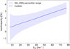 |
Fig. 16 Detector median non-linearity of the pixel response in photometric acquisition mode for SCA 18453 over all dynamical range measured during ground tests. The shadowed band extends from the 5th to the 95th percentiles of the per-pixel distribution. |
5.9.2 Reference signal definition problem
Since the definition of the reference signal Slin, as the linear coefficient of a polynomial function fitted to the ramp, could also have a number of other definitions, it deserves a few words of commentary.
For the same constant incident flux and assuming a constant baseline level, the resulting value of the reference signal depends on (1) the number and spacing of samples up the ramp, i.e. on the acquisition mode, (2) the dynamic in which the signal is measured, i.e. on the exposure time, and (3) the initial state of the detector, which may be more or less susceptible to other sources of linearity distortion, such as capture and release of charges. These differences were measured for each of the cases we analysed.
Least important is the impact of the number and spacing between UTR samples used in the polynomial fit. Whether the ramp is fitted using all the frames UTR or using several groups of 16 averaged frames, as for example in the nominal acquisition modes used by NISP, the difference does not exceed 0.1% and is usually less than 0.05% provided that the exposure time is kept constant. Between these two options we choose fitting using all the sampled frames, as it is less prone to anomalies.
More important is the dynamic that is used for the fit. In the case where the polynomial fit uses only a part of the ramp, naturally the linear coefficient will be sensitive to higher-order corrections. In our acquisition scheme for measuring non-linearity, in which several flat-field ramps are taken one after the other, fitting a polynomial to the first part of the ramp gives a higher flux estimate than an estimate based on all frames up the ramp and the same order of polynomial function. For example, the linear coefficient of 3rd order polynomial function using 76 first frames ![Mathematical equation: $\[S_{\text {lin}}^{(76)}\]$](/articles/aa/full_html/2026/03/aa55777-25/aa55777-25-eq8.png) can differ by 3% with respect to the 3 rd order polynomial function using 394 frames of the same ramp
can differ by 3% with respect to the 3 rd order polynomial function using 394 frames of the same ramp ![Mathematical equation: $\[S_{\text {lin}}^{(394)}\]$](/articles/aa/full_html/2026/03/aa55777-25/aa55777-25-eq9.png) . Interestingly, this difference is in general almost constant with flux, as illustrated in Fig. 17 by blue circles.
. Interestingly, this difference is in general almost constant with flux, as illustrated in Fig. 17 by blue circles.
The only cases in which this difference increases with flux are detectors with a large amplitude of persistence (red squares in Fig. 17). It is the continuous capture and trapping of charges, the rate of which varies depending on the state of the detector, that has the greatest impact on the linear flux estimation. A clear correlation between the non-linear reference definition and the persistence amplitude is evident while comparing the structures seen in Figs. 18 and 19. An accurate estimate of this effect in all possible acquisition schemes and in all the range of fluxes is beyond the scope of this paper. We will limit ourselves here only to point out that the measurement of non-linearity is systematically subject to error due to other physical effects present in the pixel, of which capture and emission of charges is, in our case, one of the most significant. For example, at an illumination level of about 12 000 e−, the difference in the estimation of the linear signal using a fit of a 3rd-order polynomial function to the exposure of 100 s can reach about 10% depending on the measurement scheme for detectors characterised by high persistence currents.
Therefore, to estimate the degree of non-linearity, we try to separate the effects of non-linearity from those of persistence. We use a fixed measurement scheme in which the detector is in a fixed illumination state and average the measurements over a set of exposures measured in a similar state to reduce systematic effects apart from persistence. The non-linearity is measured independently for photometric and spectrometric exposures, and the expected linear signals are calculated independently in these two schemes using the maximum number of points until the ADC saturation in each case. This measurement scheme allows us to work with a constant and stable persistence contribution. This condition will not be verified during flight. To achieve required precision, a more complex model would be required that takes both effects into account simultaneously.
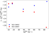 |
Fig. 17 Example of linear flux definition using ramps acquired in UTR(394). Fit performed using 76 frames |
![Mathematical equation: $\[S_{\text {lin}}^{(76)}\]$](/articles/aa/full_html/2026/03/aa55777-25/aa55777-25-eq10.png)
![Mathematical equation: $\[S_{\text {lin}}^{(394)}\]$](/articles/aa/full_html/2026/03/aa55777-25/aa55777-25-eq11.png)
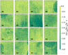 |
Fig. 18 Difference between the linear coefficient of the polynomial to the first 76 frames of the ramp with respect to the linear coefficient of the polynomial to all the 396 frames that were acquired. A correlation with the persistence map (Fig. 19) is evident. The difference in the linear flux estimate for pixels with high persistence can reach 4%. |
5.10 Persistence
Image persistence is a significant problem in infrared detectors, severely limiting data quality if its amplitude is large compared to the background level. This problem manifests itself as residual images, which can persist for several hours after observing a very bright source.
The phenomenological model explaining image persistence, proposed in Smith et al. (2008a,b), attributes it to charge trapping and release in the diode’s depletion region. Subsequent studies characterised persistence amplitudes and decay based on flux, fluence, and exposure time. Some models describe persistence decay exponentially (Serra et al. 2015; Tulloch et al. 2019; Mosby et al. 2020), while others use a power-law (Long et al. 2012; Long et al. 2015), linking it to a wide range of trapping time constants.
A comprehensive description of the persistence properties of the NISP detectors, as characterised during ground tests, is provided in Kubik et al. (2024). Here, we summarise the typical persistence amplitudes observed after non-saturating fluences and the characteristic timescale for persistence decay.
We measured the persistence current as a function of stimulus amplitudes ranging from 5000 to 95 000 e−. For each stimulus level, the persistence current was recorded during a dark exposure UTR(276), following a flat-field exposure of UTR(76). At each fluence level, the measurement was repeated 15 consecutive times.
The integrated persistence charge per pixel was determined by performing a linear fit to the dark ramp in UTR(276), multiplying the resulting slope by the typical NISP photometric exposure time, and averaging over the 15 exposures. Following a 5000 e− stimulus, the median persistence per detector ranges from 1 to 45 e−, while after a 95 000 e− stimulus (near the pixel full-well capacity of 130 000 e−), it spans from 10 to 300 e−. On average, the median persistence is below 0.3% of the stimulus for sub-saturation levels for an exposure UTR(276) directly following the stimulus (Table A.1). However, the persistence signal varies across pixels within individual detectors, as shown in Fig. 19. The dependence of the persistence amplitudes on the stimulus intensity is not linear, and the detailed description can be found in Kubik et al. (2024).
In Fig. 20, we show the decay of the persistence current measured over two hours in dark conditions. The persistence current follows a power-law decay
![Mathematical equation: $\[I(t)=I_0 t^{-\beta}\]$](/articles/aa/full_html/2026/03/aa55777-25/aa55777-25-eq12.png) (4)
(4)
for all the detectors with the average power index β = 0.72 with about 15% of dispersion between detectors. The average decay power coefficients per detector are given in Table A.1. The detailed per-pixel analysis of the power law decay is presented in Kubik et al. (2024).
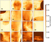 |
Fig. 19 Persistence amplitudes in percentage of the previous flat-field illumination below saturation. |
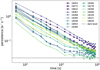 |
Fig. 20 Persistence decay over two hours after a flat-field of 80 000 e−. The lines between the dots were added to guide the eye; it is not the result of fitting the model to the data. |
6 Conclusions
The infrared detectors designed for the NISP instrument underwent a comprehensive characterisation during the TVAC campaign in 2019 in their flight configuration to ensure optimal performance for the space mission. During this process, a detailed evaluation of all key detector properties was carried out. This included identification of defective or bad pixels, evaluation of IPC, determination of gain and noise levels, measurement of dark current, and analysis of response non-linearity and persistence. As a result of these rigorous measurements, detailed detector maps were created that provide a comprehensive representation of pixel-specific properties.
The maps derived from the ground characterisation campaign serve as a reference for in-flight calibration efforts, enabling continuous monitoring and adjustment of instrument performance under operational conditions (Cogato et al. 2024). In addition, they are an essential tool for simulating instrument behaviour (Euclid Collaboration: Serrano 2024), facilitating the development and refinement of advanced data processing techniques essential for correcting data collected during instrument operation. By integrating these maps with both calibration and simulation processes, the accuracy and reliability of scientific observations is greatly enhanced, providing the high-quality data necessary to achieve the mission’s scientific goals.
Ground characterisation workflow The test results were achieved through the automated execution of a tightly designed test plan to reach the required 1% measurement precision, using advanced data acquisition software to efficiently execute the process. This automation ensured nearly 100% operational efficiency, with an extremely low failure rate, underscoring the robustness of the test structure. The tests were conducted continuously, operating 24 hours a day, 7 days a week, with minimal downtime, demonstrating the reliability of the system and its ability to maintain high performance over extended operational periods.
Detector system parameter tuning An automatic tuning procedure for all the SCS parameters was implemented and executed, significantly reducing the testing time and improving the overall efficiency of the process. The detector system operating parameters were optimised as follows: the gain was set to 15 dB, the polarisation voltage to 500 mV, and the baseline for the science pixels after reference pixel correction is in the range from 4000 to 10 000 ADU. These settings allowed the maximisation of the dynamic (excluding the DNL range), while maintaining low readout noise. The resulting dynamic was approximately 115 ke−, corresponding to a maximum measurable flux of 1000 e− s−1 in MACC(4,16,4) and 200 e− s−1 in MACC(15,16,11).
Detector system performance Regarding performance, the number of disconnected pixels was found to be minimal – fewer than 1000 per detector – and this number remained stable throughout thermal cycles, demonstrating the detectors’ reliability under varying thermal conditions. Pixels classified as inoperable accounted for less than 0.2% of the total science pixels.
The IPC coupling is minimal, with less than 1% cross-talk between neighbouring pixels. Furthermore, 95% of the pixels exhibit a QE greater than 80% across the full spectral range of the Euclid mission, indicating high sensitivity and efficient light capture.
The conversion gain is approximately 0.52 ADU/e−, with a 3% variation between detectors and less than 1% variation between channels of the same detector, ensuring consistent system response. The reset noise is approximately equal to 25 ADU and is effectively reduced to 23 ADU through reference pixel correction.
The single frame readout noise is approximately 13 e− rms, with minimal variation between detectors, ensuring consistent noise characteristics across the system. The signal estimator noise is measured at 7 e− rms in photometric mode and 9 e− rms in spectroscopic acquisition mode. The dark current is found to be below the measurement accuracy threshold.
The deviation from linear response is less than 5% for 95% of the pixels, even at signal levels up to 80 ke−, in both photometric and spectroscopic MACC modes, reflecting the high linearity of the detector’s response. The median persistence amplitude is less than 0.3% of the signal, though it exhibits significant spatial variation and differences between detectors.
Issues Achieving 1% precision per pixel necessitates exceptionally stable measurement conditions, particularly for dark current measurements, as well as a substantial volume of data to reduce statistical errors. Defining and measuring a linear signal reference for non-linearity calibration is particularly challenging in the absence of absolute calibration. The measurement duration is a crucial factor, as continuous charge capture and release affect the flux stability. The charge trapping and release have an impact on all the measurements, including the characterisation of persistence itself, adding further complexity to the analysis. Achieving the required precision in correcting for non-linearity is challenging because persistence affects the non-linearity correction, and it depends on the observation history. A model including the two effects simultaneously would be required, but is not currently available.
Calibration products, including the baseline, dead pixels, dark current, non-linearity, and persistence, were also measured under flight conditions during the early performance verification phase in 2023 and during the nominal science operations. The measurement schemes and algorithms used to generate the final maps were based on the algorithms described in this paper. The results of these measurements and their use are presented in Euclid Collaboration: Polenta (2026). The comparison with laboratory measurements is still being analysed.
Acknowledgements
The Euclid Consortium acknowledges the European Space Agency and a number of agencies and institutes that have supported the development of Euclid, in particular the Agenzia Spaziale Italiana, the Austrian Forschungsförderungsgesellschaft funded through BMK, the Belgian Science Policy, the Canadian Euclid Consortium, the Deutsches Zentrum für Luft- und Raumfahrt, the DTU Space and the Niels Bohr Institute in Denmark, the French Centre National d’Etudes Spatiales, the Fundação para a Ciência e a Tecnologia, the Hungarian Academy of Sciences, the Ministerio de Ciencia, Innovación y Universidades, the National Aeronautics and Space Administration, the National Astronomical Observatory of Japan, the Netherlandse Onderzoekschool Voor Astronomie, the Norwegian Space Agency, the Research Council of Finland, the Romanian Space Agency, the State Secretariat for Education, Research, and Innovation (SERI) at the Swiss Space Office (SSO), and the United Kingdom Space Agency. A complete and detailed list is available on the Euclid web site (www.euclid-ec.org).
References
- Bai, Y., Farris, M., Fischer, L., et al. 2018, in High Energy, Optical, and Infrared Detectors for Astronomy VIII, eds. A. D. Holland, & J. Beletic, Vol. 10709, International Society for Optics and Photonics (SPIE), 1070915 [Google Scholar]
- Barbier, R., Buton, C., Clemens, J.-C., et al. 2018, in High Energy, Optical, and Infrared Detectors for Astronomy VIII, 10709, eds. A. D. Holland, & J. Beletic, International Society for Optics and Photonics (SPIE), 107090S [Google Scholar]
- Beletic, J. W., Blank, R., Gulbransen, D., et al. 2008, in High Energy, Optical, and Infrared Detectors for Astronomy III, 7021, eds. D. A. Dorn, & A. D. Holland, International Society for Optics and Photonics (SPIE), 70210H [Google Scholar]
- Bonoli, C., Balestra, A., Bortoletto, F., et al. 2016, SPIE Conf. Ser., 9904, 99045R [Google Scholar]
- Cogato, F., Villegas, E. M., Barbier, R., et al. 2024, in Space Telescopes and Instrumentation 2024: Optical, Infrared, and Millimeter Wave, 13092, eds. L. E. Coyle, S. Matsuura, & M. D. Perrin, International Society for Optics and Photonics (SPIE), 130923G [Google Scholar]
- Costille, A., Carle, M., Fabron, C., et al. 2016, in Proceedings of SPIE – The International Society for Optical Engineering, 9904, 1996756X [Google Scholar]
- Dudik, R. P., Jordan, M. E., Dorland, B. N., et al. 2012, Appl. Opt., 51, 2877 [Google Scholar]
- Euclid Collaboration (Scaramella, R., et al.) 2022, A&A, 662, A112 [NASA ADS] [CrossRef] [EDP Sciences] [Google Scholar]
- Euclid Collaboration (Serrano, S., et al.) 2024, A&A, 690, A103 [NASA ADS] [CrossRef] [EDP Sciences] [Google Scholar]
- Euclid Collaboration (Cropper, M., et al.) 2025, A&A, 697, A2 [Google Scholar]
- Euclid Collaboration (Hormuth, F., et al.) 2025, A&A, 697, A4 [Google Scholar]
- Euclid Collaboration (Jahnke, K., et al.) 2025, A&A, 697, A3 [Google Scholar]
- Euclid Collaboration (Mellier, Y., et al.) 2025, A&A, 697, A1 [Google Scholar]
- Euclid Collaboration (Polenta, G., et al.) 2026, A&A, in press, https://doi.org/10.1051/0004-6361/202554657 [Google Scholar]
- Finger, G., Dorn, R., Meyer, M., et al. 2006, in High Energy, Optical, and Infrared Detectors for Astronomy II, 6278, eds. D. A. Dorn, & A. D. Holland, International Society for Optics and Photonics (SPIE), 62760F [Google Scholar]
- Fox, O. D., Waczynski, A., Wen, Y., et al. 2009, PASP, 121, 743 [Google Scholar]
- Holmes, W. 2019, in IOP Conf. Series: Materials Science and Engineering 101, 012024–1–8 [Google Scholar]
- Holmes, W., Aghakians, H., Avasapian, S., et al. 2022, in X-Ray, Optical, and Infrared Detectors for Astronomy X, 12191, eds. A. D. Holland, & J. Beletic, International Society for Optics and Photonics (SPIE), 121911U [Google Scholar]
- Janesick, J. R. 2007, Photon Transfer DN → λ (SPIE) [Google Scholar]
- Kubik, B., Barbier, R., Castera, A., et al. 2014, in High Energy, Optical, and Infrared Detectors for Astronomy VI, 9154, eds. A. D. Holland, & J. Beletic, International Society for Optics and Photonics (SPIE), 91541B [Google Scholar]
- Kubik, B., Barbier, R., Castera, A., et al. 2015, J. Astron. Telesc. Instrum. Syst., 1, 038001 [Google Scholar]
- Kubik, B., Barbier, R., Chabanat, E., et al. 2016, PASP, 128, 104504 [NASA ADS] [CrossRef] [Google Scholar]
- Kubik, B., Barbier, R., Smadja, G., et al. 2024, in X-Ray, Optical, and Infrared Detectors for Astronomy XI, 13103, eds. A. D. Holland, & K. Minoglou, International Society for Optics and Photonics (SPIE), 1310315 [Google Scholar]
- Laureijs, R., Amiaux, J., Arduini, S., et al. 2011, arXiv e-prints [arXiv:1110.3193] [Google Scholar]
- Le Graët, J., Secroun, A., Barbier, R., et al. 2022, SPIE Conf. Ser., 12191, 121911M [Google Scholar]
- Le Graët, J., Secroun, A., Tourneur-Silvain, M., et al. 2024, SPIE Conf. Ser., 13103, 131031W [Google Scholar]
- Long, K. S., Baggett, S. M., MacKenty, J. W., & Riess, A. G. 2012, in Space Telescopes and Instrumentation 2012: Optical, Infrared, and Millimeter Wave, 8442, eds. M. C. Clampin, G. G. Fazio, H. A. MacEwen, & J. M. Oschmann Jr., International Society for Optics and Photonics (SPIE), 84421W [Google Scholar]
- Long, K. S., Baggett, S. M., & MacKenty, J. W. 2015, Persistence in the WFC3 IR Detector: An Improved Model Incorporating the Effects of Exposure Time, WFC3 Instrument Science Report 2015-15 [Google Scholar]
- Loose, M., Beletic, J., Blackwell, J., et al. 2005, in Cryogenic Optical Systems and Instruments XI, 5904, eds. J. B. Heaney, & L. G. Burriesci, International Society for Optics and Photonics (SPIE), 59040V [Google Scholar]
- Loose, M., Beletic, J., Garnett, J., & Xu, M. 2007, in Focal Plane Arrays for Space Telescopes III, 6690, eds. T. J. Grycewicz, C. J. Marshall, & P. G. Warren, International Society for Optics and Photonics (SPIE), 66900C [Google Scholar]
- Maciaszek, T., Ealet, A., Gillard, W., et al. 2022, SPIE Conf. Ser., 12180, 121801K [NASA ADS] [Google Scholar]
- Medinaceli, E., Farinelli, R., Balestra, A., et al. 2020, SPIE Conf. Ser., 11443, 1144359 [Google Scholar]
- Moore, A. C., Ninkov, Z., & Forrest, W. J. 2004, SPIE Conf. Ser., 5167, 204 [NASA ADS] [Google Scholar]
- Moore, A. C., Ninkov, Z., & Forrest, W. J. 2006, Opt. Eng., 45, 076402 [Google Scholar]
- Mosby, G., Rauscher, B. J., Bennett, C., et al. 2020, J. Astron. Telesc. Instrum. Syst., 6, 046001 [Google Scholar]
- Moseley, S. H., Arendt, R. G., Fixsen, D. J., et al. 2010, in Proceedings of the SPIE, eds. A. D. Holland, & D. A. Dorn, NASA Goddard Space Flight Ctr., United States (SPIE), 77421B [Google Scholar]
- Plazas, A. A., Shapiro, C., Smith, R., Rhodes, J., & Huff, E. 2017, J. Instrum., 12, C04009 [NASA ADS] [CrossRef] [Google Scholar]
- Rauscher, B. J., Fox, O., Ferruit, P., et al. 2007, PASP, 119, 768 [NASA ADS] [CrossRef] [Google Scholar]
- Rauscher, B. J., Arendt, R. G., Fixsen, D. J., et al. 2017, PASP, 129, 105003 [NASA ADS] [CrossRef] [Google Scholar]
- Secroun, A., Barbier, R., Buton, C., et al. 2018, SPIE Conf. Ser., 10709, 1070921 [Google Scholar]
- Secroun, A., Serra, B., Clémens, J. C., et al. 2016, SPIE Conf. Ser., 9915, 99151Y [Google Scholar]
- Serra, B., Secroun, A., Clémens, J.-C., et al. 2015, in UV/Optical/IR Space Telescopes and Instruments: Innovative Technologies and Concepts VII, 9602, eds. H. A. MacEwen, & J. B. Breckinridge, International Society for Optics and Photonics (SPIE), 96020G [Google Scholar]
- Smith, R. M., Zavodny, M., Rahmer, G., & Bonati, M. 2008a, in High Energy, Optical, and Infrared Detectors for Astronomy III, 7021, eds. D. A. Dorn, & A. D. Holland, International Society for Optics and Photonics (SPIE), 70210J [Google Scholar]
- Smith, R. M., Zavodny, M., Rahmer, G., & Bonati, M. 2008b, in High Energy, Optical, and Infrared Detectors for Astronomy III, 7021, eds. D. A. Dorn, & A. D. Holland, International Society for Optics and Photonics (SPIE), 70210K [Google Scholar]
- Tulloch, S., George, E., & Group, E. D. S. 2019, J. Astron. Telesc. Instrum. Syst., 5, 036004 [Google Scholar]
- Vacca, W. D., Cushing, M. C., & Rayner, J. T. 2004, PASP, 116, 352 [Google Scholar]
- Waczynski, A., Barbier, R., Cagiano, S., et al. 2016, in High Energy, Optical, and Infrared Detectors for Astronomy VII, 9915, eds. A. D. Holland, & J. Beletic, International Society for Optics and Photonics (SPIE), 991511 [Google Scholar]
- Williams, M., Benfield, C., Warner, B., et al. 2019, Expert Twisted: EventDriven and Asynchronous Programming with Python, 1st edn. (Berkeley, CA: Apress), XIX, 382 [Google Scholar]
HAWAII is an acronym for HgCdTe Astronomical Wide Area Infrared Imager. It includes a family of HxRG detectors, where H stands for HAWAII, the number x=1, 2, 4 denotes 1024 × 1024, 2048 × 2048 or 4096 × 4096 pixels, R stands for reference pixels, and G for guide window capability.
Baseline is defined as the average value of the first 16 frames after a pixel reset.
The ROIC and SIDECAR ASIC clock all frames and transmit all data to the warm readout electronics in order to maintain thermal stability of the SCAs and SCEs. Selection of frames to coadd or drop is performed in the warm electronics.
CDS involves resetting the detector array and then reading it at least twice, generating two frames at an interval of at least one frame.
The preamplifier provides control over the gain and bandwidth of the analogue signal using programmable capacitors and resistors. Preamplifier gain is not the same parameter as the conversion gain, described in Sect. 5.6.
This was a phase that lasted from 2012 to 2015. During this phase, pre-development versions of SCS parts were designed, manufactured, qualified, and evaluated for performance. The phase ended with approval for production of the flight parts.
H2RG can interleave the readout of the guiding window with the readout of the entire array, so that the science array can perform the guiding function required to accurately stabilise the telescope (Beletic et al. 2008).
Appendix A Detector properties summary table
H2RG median properties from ground characterisations across the NISP focal plane. dpix – number of disconnected pixels, BR – baseline of reference pixels, B – baseline of science pixels, RNc – reset noise after reference pixel subtraction, QE[YE,JE,HE] – quantum efficiency in % in three photometric bands, IPC – central pixel value of the interpixel capacitance kernel [%], CG – conversion gain, σR – single frame readout noise after reference pixel correction, dph, dsp – dark currents measured in photomeric and spectroscopic integration times at 80 000 integrated electrons, σph – noise of signal estimator in MACC(4,16,4), σsp – noise of signal estimator in MACC(15, 16, 11), nl – departure from linearity at 80 000 integrated electrons in MACC(4,16,4), pers – persistence amplitude as percentage of 80 ke− flat-field intensity, β – persistence decay power index.
Appendix B Data-based orthogonal polynomials formalism
We have a vector of dimension D of measurement points xi = {x1, x2, . . ., xD} and the vector of measured values yi(xi) = {y1, y2,. . ., yD}; for example, in an UTR(400) exposure, xi would be the frame number xi = {1, 2,. . ., 400} and yi would correspond to the ADU read in the pixel at each frame, yi(xi) = {100, 200,. . ., 40 000}.
The pixel response is non-linear, and we assume that it can be modelled by a polynomial of order N:
![Mathematical equation: $\[y(x)=\sum_{i=0}^N \beta_i x^i.\]$](/articles/aa/full_html/2026/03/aa55777-25/aa55777-25-eq13.png) (B.1)
(B.1)
Then we choose to decompose the function y(x) on the basis of orthogonal polynomials Pi(x),
![Mathematical equation: $\[y(x)=\sum_{i=0}^N \alpha_i P_i(x),\]$](/articles/aa/full_html/2026/03/aa55777-25/aa55777-25-eq14.png) (B.2)
(B.2)
where Pi(x) is a polynomial of order i, defined as
![Mathematical equation: $\[P_i(x)=\sum_{j=0}^i a_{i j} x^i.\]$](/articles/aa/full_html/2026/03/aa55777-25/aa55777-25-eq15.png) (B.3)
(B.3)
By identifying the coefficients in front of the j-th power of x in Eqns. (B.1) and (B.2) we get the expression of βj as a function of αi and aij:
![Mathematical equation: $\[\beta_j=\sum_{i=j}^N \alpha_i a_{i j}.\]$](/articles/aa/full_html/2026/03/aa55777-25/aa55777-25-eq16.png) (B.4)
(B.4)
Physically β0 corresponds to the pixel baseline [ADU], β1 is the expected linear flux value [ADU/frame] and βi>1 are the terms that describe the deviations from the ideal linear response of the pixel to a constant incident flux [βj] =ADU/framej.
The problem is to find the set of coefficients βj that fits the pixel response, so to find αis and aijs with i, j ∈ 1 . . .N. Below we present the formulas to compute αis and aijs given measurement xi = {x1, x2, . . ., xD} and yi(xi) = {y1, y2,. . ., yD}. The coefficients aij of each polynomial Pi(x) are computed using the orthogonality and normalisation conditions on xi = {x1, x2, . . ., xD}
![Mathematical equation: $\[\left\langle P_m, P_n\right\rangle \equiv \sum_{i=1}^D P_m(x_i) P_n(x_i)=\delta_{m n}.\]$](/articles/aa/full_html/2026/03/aa55777-25/aa55777-25-eq17.png) (B.5)
(B.5)
For m > n this gives
![Mathematical equation: $\[\left\langle P_m, P_n\right\rangle=\sum_{i=1}^D P_m(x_i) P_n(x_i)=\sum_{k=0}^m a_{m k} \gamma_{n k}.\]$](/articles/aa/full_html/2026/03/aa55777-25/aa55777-25-eq18.png) (B.6)
(B.6)
Dividing the above equation by am0 and defining ![Mathematical equation: $\[a_{m j}^{\prime}=\frac{a_{m j}}{a_{m 0}}\]$](/articles/aa/full_html/2026/03/aa55777-25/aa55777-25-eq19.png) we get
we get
![Mathematical equation: $\[0=\gamma_{n 0}+a_{m 1}^{\prime} \gamma_{n 1}+a_{m 2}^{\prime} \gamma_{n 2}+\cdots+a_{m m}^{\prime} \gamma_{n m}.\]$](/articles/aa/full_html/2026/03/aa55777-25/aa55777-25-eq20.png) (B.7)
(B.7)
Considering the orthogonality of Pm to all Pn with n < m (Pn = {P0, P1, . . ., Pm–1}) we construct a system of m linear equations with m unknowns ![Mathematical equation: $\[a_{m j}^{\prime}\]$](/articles/aa/full_html/2026/03/aa55777-25/aa55777-25-eq21.png) with j = 1 . . . m,
with j = 1 . . . m,
![Mathematical equation: $\[\begin{aligned}& \left\langle P_n, P_m\right\rangle \\& \left\langle P_0, P_m\right\rangle \Rightarrow \\& \left\langle P_1, P_m\right\rangle \Rightarrow \\& \left\langle P_2, P_m\right\rangle \Rightarrow \\& \left\langle P_{m-1}, P_m\right\rangle \Rightarrow\end{aligned} \quad\left(\begin{array}{ccccc}j=1 & j=2 & \ldots & j=m & \\\gamma_{01} a_{m 1}^{\prime} & \gamma_{02} a_{m 2}^{\prime} & \ldots & \gamma_{0 m} a_{m m}^{\prime} & =\gamma_{00} \\\gamma_{11} a_{m 1}^{\prime} & \gamma_{12} a_{m 2}^{\prime} & \ldots & \gamma_{1 m} a_{m m}^{\prime} & =\gamma_{10} \\\gamma_{21} a_{m 1}^{\prime} & \gamma_{22} a_{m 2}^{\prime} & \ldots & \gamma_{2 m} a_{m m}^{\prime} & =\gamma_{20} \\& a_{m 2}^{\prime} & \ldots & & \\\gamma_{m-1,1} a_{m 1}^{\prime} & \gamma_{m-1,2} a_{m 2}^{\prime} & \ldots & \gamma_{m-1, m} a_{m m}^{\prime} & =\gamma_{m-1,0}\end{array}\right).\]$](/articles/aa/full_html/2026/03/aa55777-25/aa55777-25-eq22.png) (B.8)
(B.8)
The system can be easily solved by any well established method. We propose the determinant method. To find ![Mathematical equation: $\[a_{m j}^{\prime}\]$](/articles/aa/full_html/2026/03/aa55777-25/aa55777-25-eq23.png) we compute the determinant of the matrix Γ,
we compute the determinant of the matrix Γ,
![Mathematical equation: $\[\Gamma=\left(\begin{array}{cccccc}\gamma_{01} & \gamma_{02} & \cdots & \gamma_{0 j} & \cdots & \gamma_{0 m} \\\gamma_{11} & \gamma_{12} & \cdots & \gamma_{1 j} & \cdots & \gamma_{1 m} \\\gamma_{21} & \gamma_{22} & \cdots & \gamma_{2 j} & \cdots & \gamma_{2 m} \\\vdots & \vdots & \vdots & \vdots & \ddots & \vdots \\\gamma_{m-1,1} & \gamma_{m-1,2} & \cdots & \gamma_{m-1, j} & \cdots & \gamma_{m-1, m}\end{array}\right),\]$](/articles/aa/full_html/2026/03/aa55777-25/aa55777-25-eq24.png) (B.9)
(B.9)
and the determinant of Γj where the j-th column of Γ was replaced by the vector of free terms {γ00 . . . γm–1,0},
![Mathematical equation: $\[\Gamma_j=\left(\begin{array}{cccccc}\gamma_{01} & \gamma_{02} & \cdots & \gamma_{00} & \cdots & \gamma_{0 m} \\\gamma_{11} & \gamma_{12} & \cdots & \gamma_{10} & \cdots & \gamma_{1 m} \\\gamma_{21} & \gamma_{22} & \cdots & \gamma_{20} & \cdots & \gamma_{2 m} \\\vdots & \vdots & \vdots & \vdots & \ddots & \vdots \\\gamma_{m-1,1} & \gamma_{m-1,2} & \cdots & \gamma_{m-1,0} & \cdots & \gamma_{m-1, m}\end{array}\right).\]$](/articles/aa/full_html/2026/03/aa55777-25/aa55777-25-eq25.png) (B.10)
(B.10)
The solution for ![Mathematical equation: $\[a_{m j}^{\prime}\]$](/articles/aa/full_html/2026/03/aa55777-25/aa55777-25-eq26.png) is then:
is then:
![Mathematical equation: $\[a_{m j}^{\prime}=\frac{\operatorname{det} \Gamma_j}{\operatorname{det} \Gamma}.\]$](/articles/aa/full_html/2026/03/aa55777-25/aa55777-25-eq27.png) (B.11)
(B.11)
The absolute scale of the coefficients ami is found by considering the normalisation of Pm(x)
![Mathematical equation: $\[\left\langle P_m, P_m\right\rangle=\sum x^{i+j},\]$](/articles/aa/full_html/2026/03/aa55777-25/aa55777-25-eq28.png) (B.12)
(B.12)
from which we have
![Mathematical equation: $\[\begin{aligned}&a_{m 0}=\left(\sum_{i=0}^N\left(a_{m i}^{\prime 2} \sum x^{2 i}\right)+2 a_{m i}^{\prime} \sum_{j=i+1}^N a_{m j}^{\prime} \sum x^{i+j}\right)^{-1 / 2}\end{aligned}\]$](/articles/aa/full_html/2026/03/aa55777-25/aa55777-25-eq29.png) (B.13)
(B.13)
and
![Mathematical equation: $\[a_{m j}=a_{m j}^{\prime} a_{m 0}.\]$](/articles/aa/full_html/2026/03/aa55777-25/aa55777-25-eq30.png) (B.14)
(B.14)
The coefficients αi are found by projecting the measurements yi on the basis of the orthogonal polynomials:
![Mathematical equation: $\[\alpha_m=\left\langle y, P_m\right\rangle=\sum_{i=1}^D y_i P_m\left(x_i\right)=\sum_{i=1}^D y_i \sum_{j=0}^m a_{m j} x_i^j.\]$](/articles/aa/full_html/2026/03/aa55777-25/aa55777-25-eq31.png) (B.15)
(B.15)
In summary, in order to fit the data using orthogonal polynomials one needs to do the following:
Compute aij using Eqs. (B.11), (B.13), and (B.14). It is common for all the pixels, as it depends only on the time coordinates x.
Compute αi using Eq. (B.15). This quantity is pixel dependent as it depends linearly on the pixel signal values y.
Compute βj using Eq. (B.4).
This method offers a significant advantage over traditional numerical fitting approaches, particularly when applied to a dataset of this magnitude (involving independent fits for 2040 × 2040 pixels by 16 detectors across numerous fluence levels). The key benefit lies in the pre-computation of the aij coefficients for the entire dataset. Once these coefficients are determined, the computation is greatly simplified to straightforward multiplications of per-pixel signal values to calculate αij. This makes the method highly efficient and scalable for large datasets.
All Tables
NISP acquisition modes, MACC(ng, nf, nd), and corresponding UTR(n) used during ground characterisations with n = nfng + nd(ng − 1).
Bad pixel budget per detector as measured during ground tests. In the last row the combined total, excluding double-counting, is given.
Percentiles (5th, 50th, and 95th) of the average QE in the NISP photometric bands YE, JE, and HE.
Percentiles (5th, 50th, and 95th) of non-linearity at 80 000 integrated electrons in photometric and spectroscopic exposure time.
H2RG median properties from ground characterisations across the NISP focal plane. dpix – number of disconnected pixels, BR – baseline of reference pixels, B – baseline of science pixels, RNc – reset noise after reference pixel subtraction, QE[YE,JE,HE] – quantum efficiency in % in three photometric bands, IPC – central pixel value of the interpixel capacitance kernel [%], CG – conversion gain, σR – single frame readout noise after reference pixel correction, dph, dsp – dark currents measured in photomeric and spectroscopic integration times at 80 000 integrated electrons, σph – noise of signal estimator in MACC(4,16,4), σsp – noise of signal estimator in MACC(15, 16, 11), nl – departure from linearity at 80 000 integrated electrons in MACC(4,16,4), pers – persistence amplitude as percentage of 80 ke− flat-field intensity, β – persistence decay power index.
All Figures
|
Fig. 1 Photo of a Euclid-like engineering grade sensor chip system taken in the clean room of the CNRS-IN2P3 Center for Particle Physics in Marseille (CPPM). The sensitive surface is 3.6 cm × 3.6 cm. Credit: CPPM-CNRS. |
| In the text | |
|
Fig. 2 Illustration of the multi-accumulation acquisition mode MACC(ng, nf, nd) with ng = 4, nf = 16, nd = 4 and one reset frame. The integration time tint and exposure time texp defined in Eqs. (1) and (2), respectively, are also indicated. |
| In the text | |
|
Fig. 3 H2RG frame geometry definition with reference pixels on the edges of the array in the 32-output channel mode. The read directions are indicated by the blue arrows. The widths are not in scale. |
| In the text | |
|
Fig. 4 TV workflow as implemented and executed during the 14-day testing period. In the boxes we specify the type of test, the test duration in hours, and the range of fluxes that were used. No indication of flux values means that the test was performed in dark conditions. All tests were performed with a 99.73% time efficiency. |
| In the text | |
|
Fig. 5 Hierarchical data structure defined for the SCS characterisation campaign. |
| In the text | |
|
Fig. 6 Baseline image of the whole FPA before reference pixel correction. This and all subsequent detector maps are displayed in the R-MOSAIC coordinate system (Euclid Collaboration: Jahnke 2025). |
| In the text | |
|
Fig. 7 Distribution of the baseline values after reference pixel correction. The black dots represent the 5th, 50th, and 95th percentiles of the science pixels baseline distribution. |
| In the text | |
|
Fig. 8 Example of the spatial distribution of bad pixels across an array. |
| In the text | |
|
Fig. 9 Map of the central pixel value of the IPC kernel. The void regions are visible as yellow shapes. |
| In the text | |
|
Fig. 10 Mean IPC kernel per detector with sub-percent accuracy. |
| In the text | |
|
Fig. 11 Map of the average QE in the NISP JE band (1168–1567 nm). |
| In the text | |
|
Fig. 12 QE as a function of wavelength. The points indicate the lowest 5th percentile per detector. 95% of the pixels have QE values higher than 80% over most of the wavelength range. |
| In the text | |
|
Fig. 13 Conversion gain per channel computed using flat-field ramps with increasing (IR3 < IR4 < IR5) illumination levels. In the legends for each detector the average gain over the 32 channels and the dispersion between channels are given. For all the three illuminations the mean conversion gain for the whole FPA is 0.52 ADU/e− with a 3% variation between arrays. The channel-to-channel gain variation inside a detector is less than 1%. The gain variation with signal is described in Le Graët et al. (2024). |
| In the text | |
|
Fig. 14 Reset noise of science pixels before (blue circles) and after (red triangles) reference pixel correction. The reset noise of reference pixels is shown as green circles. For each detector in the legend the average reset noise over the 32 channels is indicated, and in parentheses the relative dispersion of the average reset noise between channels is given. At the top (in the title) we indicate the average reset noise over the whole FPA and the dispersion between detectors before reference pixel correction. The values after reference pixel correction are given in brackets. |
| In the text | |
|
Fig. 15 Cumulative distributions of single frame readout noise for the 16 detector arrays after reference pixel correction. The black dots represent the 5th, 50th, and 95th percentiles of the distribution. |
| In the text | |
|
Fig. 16 Detector median non-linearity of the pixel response in photometric acquisition mode for SCA 18453 over all dynamical range measured during ground tests. The shadowed band extends from the 5th to the 95th percentiles of the per-pixel distribution. |
| In the text | |
|
Fig. 17 Example of linear flux definition using ramps acquired in UTR(394). Fit performed using 76 frames |
| In the text | |
|
Fig. 18 Difference between the linear coefficient of the polynomial to the first 76 frames of the ramp with respect to the linear coefficient of the polynomial to all the 396 frames that were acquired. A correlation with the persistence map (Fig. 19) is evident. The difference in the linear flux estimate for pixels with high persistence can reach 4%. |
| In the text | |
|
Fig. 19 Persistence amplitudes in percentage of the previous flat-field illumination below saturation. |
| In the text | |
|
Fig. 20 Persistence decay over two hours after a flat-field of 80 000 e−. The lines between the dots were added to guide the eye; it is not the result of fitting the model to the data. |
| In the text | |
Current usage metrics show cumulative count of Article Views (full-text article views including HTML views, PDF and ePub downloads, according to the available data) and Abstracts Views on Vision4Press platform.
Data correspond to usage on the plateform after 2015. The current usage metrics is available 48-96 hours after online publication and is updated daily on week days.
Initial download of the metrics may take a while.